Semiconductor package

A technology for semiconductors and packages, which is applied in the field of fan-out semiconductor packages, and can solve problems such as reduced insulation reliability and differences

Inactive Publication Date: 2020-05-05
SAMSUNG ELECTRONICS CO LTD
View PDF1 Cites 0 Cited by
  • Summary
  • Abstract
  • Description
  • Claims
  • Application Information

AI Technical Summary

Problems solved by technology

[0005] However, when the coating method is applied, the substrate may be coated along the pattern shape, which may cause a gap between the thickness of the insulating layer in the region covering the pattern already formed on the substrate and the thickness of the insulating layer between the patterns. There may be fluctuations in the difference
If the fluctuation increases, the insulation reliability may decrease

Method used


Image

  • Semiconductor package
  • Semiconductor package
  • Semiconductor package

Examples


Embodiment Construction

[0021] Hereinafter, example embodiments of the present disclosure will be described with reference to the accompanying drawings. In the drawings, the shapes, dimensions, etc. of elements may be exaggerated or briefly shown for clarity of description.

[0022] electronic device

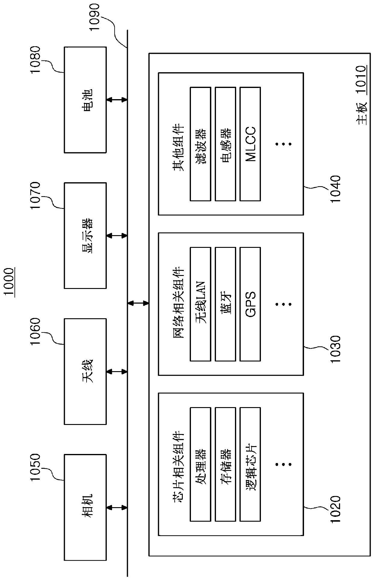
[0023] figure 1 is a schematic block diagram illustrating an example of an electronic device system.

[0024] refer to figure 1 , the electronic device 1000 may accommodate the motherboard 1010 therein. The motherboard 1010 may include chip-related components 1020 , network-related components 1030 , other components 1040 , etc., physically connected or electrically connected thereto. These components may be connected to other components to be described below through various signal lines 1090 .

[0025] Chip-related components 1020 may include: memory chips, such as volatile memory (eg, dynamic random access memory (DRAM)), non-volatile memory (eg, read-only memory (ROM)), flash memory, etc.; app...


PUM


Abstract

The invention provides a semiconductor package. The semiconductor package includes a semiconductor chip having a connection pad; an encapsulant covering at least a portion of the semiconductor chip; and an interconnect structure disposed on the semiconductor chip and the encapsulant. The interconnect structure includes a first insulating layer, a first redistribution layer disposed on the first insulating layer, and a second insulating layer disposed on the first insulating layer and covering the first redistribution layer, the first redistribution layer is electrically connected to the connection pad, and when a thickness of the first redistribution layer is a, and a gap between patterns of the first redistribution layer is b, b / a is 4 or less.

Description

[0001] This application claims the benefit of priority from Korean Patent Application No. 10-2018-0129208 filed on October 26, 2018 at the Korean Intellectual Property Office, the disclosure of which is hereby incorporated by reference in its entirety. technical field [0002] The present disclosure relates to a semiconductor package, and more particularly, to a fan-out type semiconductor package. Background technique [0003] One of the main trends in the field of semiconductor technology is to reduce the size of components, and according to the increase in consumption of small-sized semiconductor chips in the field of package development, there has been a need to realize multiple pins with reduced sizes. In order to meet the demand, fan-out type semiconductor packages have been developed. In fan-out semiconductor packages, connection pads (pads, or "pads" or "bonding pads") can be redistributed to areas other than the area where the semiconductor chip is disposed, so that ...

Claims


Application Information

Patent Timeline
IPC IPC(8): H01L23/48H01L23/525H01L23/528H01L23/31
CPCH01L23/3121H01L23/481H01L23/525H01L23/528H01L23/13H01L23/3128H01L23/49816H01L23/49822H01L23/49833H01L23/5389H01L2224/18H01L23/04H01L23/31H01L23/485H01L24/05H01L2224/02379H01L23/053H01L23/49838
Inventor 徐永官文昭渊蔡昇训
Owner SAMSUNG ELECTRONICS CO LTD
Why Eureka
Try Eureka