Preparation method and application of MEMS infrared light source

An infrared light source and infrared light technology, applied in the field of infrared light source, can solve problems such as high integration difficulty, high application cost, and difficulty in heat dissipation of the light source, and achieve the effects of reducing integration difficulty, improving generation efficiency, and ensuring thermal insulation performance

Active Publication Date: 2020-05-08
HUAZHONG UNIV OF SCI & TECH
View PDF5 Cites 1 Cited by
  • Summary
  • Abstract
  • Description
  • Claims
  • Application Information

AI Technical Summary

Problems solved by technology

[0005] The invention provides a method for preparing a MEMS infrared light source and its application, which is used to solve the technical problems of high integration difficulty and high application cost due to the adoption of a front-emitting structure of the existing MEMS infrared light source in integrated applications

Method used


Image

  • Preparation method and application of MEMS infrared light source
  • Preparation method and application of MEMS infrared light source
  • Preparation method and application of MEMS infrared light source

Examples


Embodiment 1

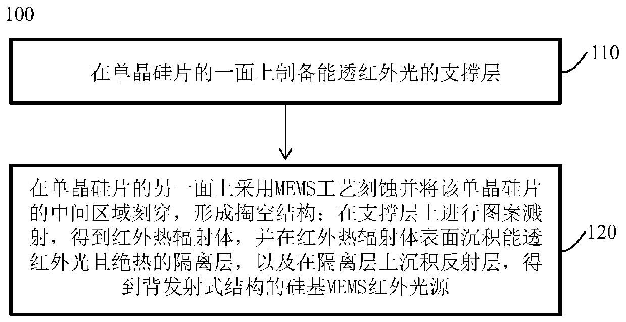
[0035] A preparation method 100 of a MEMS infrared light source, such as figure 1 shown, including:

[0036] Step 110, preparing a support layer capable of transmitting infrared light on one side of the single crystal silicon wafer;

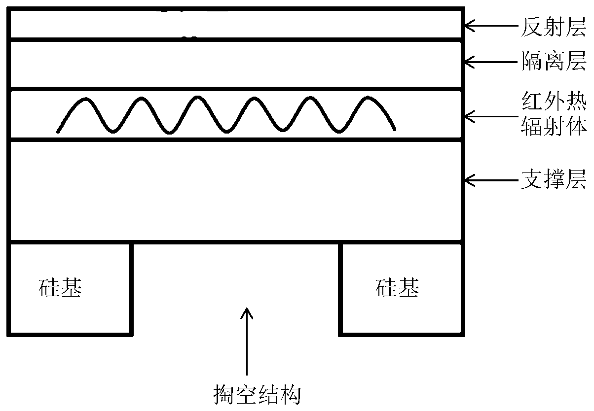
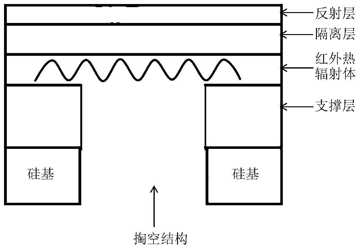
[0037] Step 120, using MEMS technology to etch the other side of the single crystal silicon wafer and carving through the middle area of ​​the single crystal silicon wafer to form a hollow structure; performing pattern sputtering on the support layer to obtain an infrared heat radiator, And on the surface of the infrared heat radiator, an isolation layer capable of transmitting infrared light and heat insulation is deposited, and a reflective layer is deposited on the isolation layer to obtain a silicon-based MEMS infrared light source with a back-emitting structure.

[0038] It should be noted that in step 120, the MEMS process is used to etch to form a hollow structure and pattern sputtering on the support layer. There is no necessary sequence...

Embodiment 2

[0105] A MEMS infrared light source device, comprising: a MEMS infrared light source prepared by any one of the MEMS infrared light source preparation methods described in the first embodiment above, and a power supply electrically connected to the infrared heat radiator in the light source.

[0106] The heating wire (such as Pt) is used as the radiation source, the upper layer of silicon nitride is used as the isolation layer (which acts as a thermal insulation and isolates the heating wire and the reflective layer), and the gold layer is used as the reflective layer. The reflectivity of gold reaches 99%, which can almost completely reflect All the infrared light radiated by the heating wire is radiated from the cavity of the silicon on the back to form a back-emitting MEMS infrared light source. The prepared back-emitting MEMS infrared light source can not only reduce the loss of radiated light from black body radiation, but also enhance the intensity of the light source, and...

Embodiment 3

[0109] An infrared detection integrated system, comprising: a MEMS infrared light source device as described in the second embodiment above, and its corresponding back-end infrared receiving device, wherein, the edge of the hollowed out structure in the infrared light source device and the infrared receiving device Infrared light input port connection.

[0110] For example, the NDIR infrared gas sensor based on the non-dispersive infrared (Non-Dispersive Infra-Red, NDIR) absorption principle is based on the near-infrared spectrum selective absorption characteristics of different gas molecules, using the relationship between gas concentration and absorption intensity (Lambert-Beer’s law) A gas sensing device that identifies gas components and determines their concentrations. Current NDIR infrared gas sensors are usually composed of discrete components such as a light source, a gas chamber, and a detector. According to the NDIR measurement principle, the sensitivity, detection ...


PUM


Abstract

The invention belongs to the field of infrared light sources, and particularly discloses a preparation method and application of an MEMS infrared light source, and the preparation method comprises thesteps: preparing a supporting layer capable of transmitting infrared light on one surface of a monocrystalline silicon wafer; etching the other surface of the monocrystalline silicon wafer by adopting an MEMS process and etching through the middle area of the monocrystalline silicon wafer to form a hollowed-out structure; and performing pattern sputtering on the support layer to obtain an infrared heat radiator, depositing an infrared-light-transmitting and heat-insulating isolation layer on the surface of the infrared heat radiator, and depositing a reflection layer on the isolation layer toobtain the silicon-based MEMS infrared light source with the back-emitting structure. After the supporting layer is arranged on one side of the monocrystalline silicon wafer, MEMS process etching iscarried out on the other side of the monocrystalline silicon wafer to form the hollowed-out structure with the edge being a silicon substrate and the middle area being etched through, and meanwhile, the infrared heat radiator, the isolation layer and the reflection layer are sequentially arranged on the supporting layer. The back emission type infrared light source prepared by the method is high in infrared emission efficiency, and can effectively reduce the integration difficulty and the integration cost in application.

Description

technical field [0001] The invention belongs to the field of infrared light sources, and more specifically relates to a method for preparing a MEMS infrared light source and an application thereof. Background technique [0002] Infrared light source is a non-illumination light source that generates heat by Joules and radiates infrared light. It has the advantages of strong anti-interference ability, good environmental adaptability, high spatial resolution and sensitivity. It is mainly used in infrared imaging, infrared remote control, inspection of metal wires, Internal inspection of plastic bottles and other fields. Traditional infrared light sources generally need to use a chopper to modulate the infrared signal, which limits the development of portability, integration, and low power consumption. The development of MEMS (Micro Electro Mechanical Systems, Micro Electro Mechanical Systems) technology has promoted the development of electrically adjustable infrared light sou...

Claims


Application Information

Patent Timeline
Patent Type & Authority Applications(China)
IPC IPC(8): B81C1/00B81B7/00B81B7/02G01J5/20G01N21/3504
CPCB81C1/00349B81C1/00523B81B7/02B81B7/0019B81B7/0087G01N21/3504G01J5/20Y02P70/50
Inventor 刘欢唐江易飞田枝来胡志响严棋陈浩
Owner HUAZHONG UNIV OF SCI & TECH
Why Eureka
Try Eureka