Packaging structure of igbt chip subunit and manufacturing method thereof

A technology of packaging structure and manufacturing method, applied in semiconductor/solid-state device manufacturing, electrical components, semiconductor/solid-state device components, etc.

Active Publication Date: 2021-06-08
ZHUZHOU CRRC TIMES SEMICON CO LTD
View PDF10 Cites 0 Cited by
  • Summary
  • Abstract
  • Description
  • Claims
  • Application Information

AI Technical Summary

Problems solved by technology

[0006] In view of the shortcomings of the above packaging methods, a new packaging method is proposed to protect the chip terminals from electrical breakdown caused by pollution.

Method used


Image

  • Packaging structure of igbt chip subunit and manufacturing method thereof
  • Packaging structure of igbt chip subunit and manufacturing method thereof
  • Packaging structure of igbt chip subunit and manufacturing method thereof

Examples


Embodiment Construction

[0035] The present invention will be further described below in conjunction with accompanying drawing.

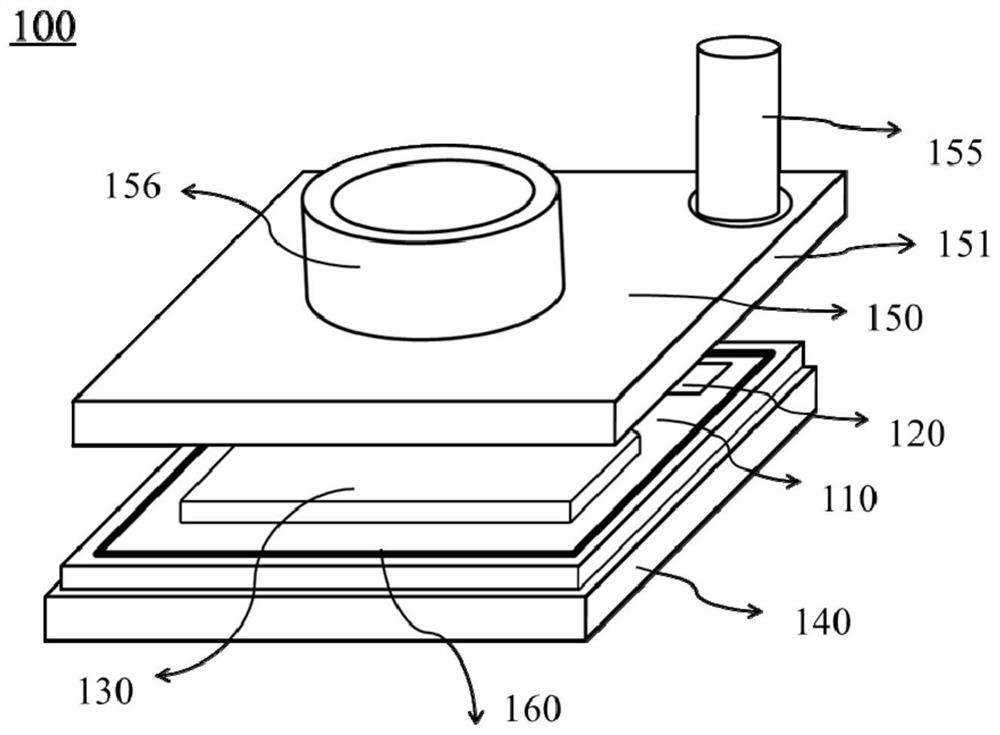
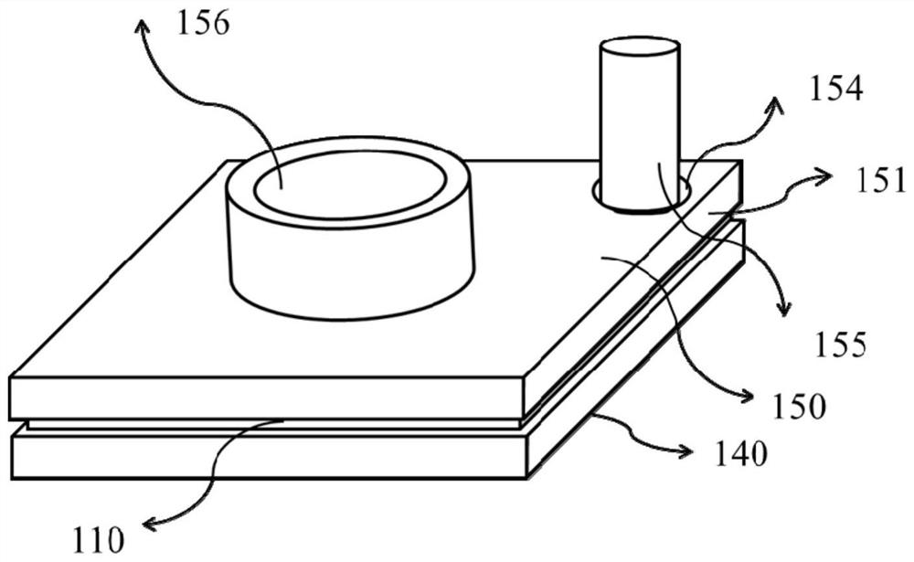
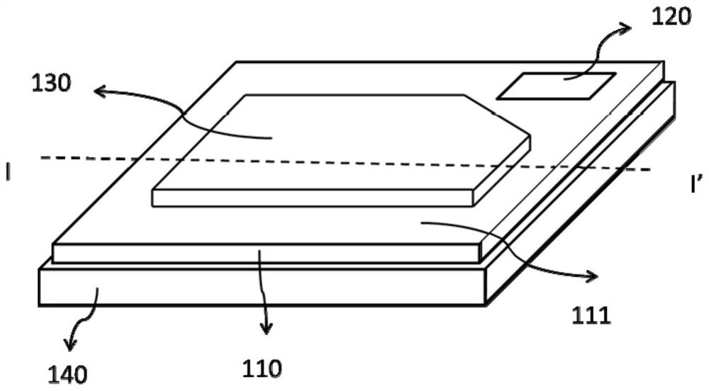
[0036] figure 1 and figure 2 It is a schematic structural diagram of the IGBT chip subunit packaging structure 100 provided in this application. like figure 1 and figure 2 As shown, the packaging structure 100 includes an IGBT chip 110, a gate 120 disposed on the IGBT chip, an upper molybdenum sheet 130 and a lower molybdenum sheet 130 electrically connected to the upper surface emitter 111 and the lower surface collector 112 of the IGBT chip 110 respectively. The chip 140 and the encapsulator 150 are coated with silicon rubber 160 on the emitter electrode 111 on the upper surface and along the terminal area 113 of the IGBT chip 110 .

[0037] Through the packaging structure of the IGBT chip subunit provided in this application, the terminal structure of the IGBT chip can be passivated and protected, preventing electrical breakdown caused by contamination of the chip ...


PUM


Abstract

The present application provides an IGBT chip sub-unit packaging structure and a manufacturing method thereof. The packaging structure includes an IGBT chip, a gate arranged on the IGBT chip, and an electrode connected to the upper surface emitter and the lower surface collector of the IGBT chip respectively. The connected upper molybdenum sheet and lower molybdenum sheet and the encapsulator, wherein the emitter on the upper surface is coated with silicon rubber along the terminal area of ​​the IGBT chip. Through the packaging structure of the present application and its manufacturing method, the terminal structure of the IGBT chip can be protected by passivation, which avoids electrical breakdown caused by contamination of the chip terminal by external factors, and improves the voltage resistance of the chip and the reliability of long-term work. sex.

Description

technical field [0001] The present invention relates to the field of power semiconductor devices, and more specifically, relates to a packaging structure of an IGBT chip subunit and a manufacturing method thereof. Background technique [0002] The power semiconductor device IGBT, that is, the insulated gate bipolar transistor, is a power electronic device combined with a MOS field effect structure and a bipolar transistor. Large and other advantages, it is widely used in rail transit, smart grid and industrial transmission fields. The packaging forms of IGBT modules include the traditional soldering type and the new crimping type, among which the crimping type packaging has the advantages of high power density, double-sided heat dissipation, and high reliability. [0003] The press-fit IGBT module forms an internal interconnection between the IGBT and (or) the anti-parallel FRD chip, the molybdenum sheet, and the upper and lower electrodes through external physical pressure...

Claims


Application Information

Patent Timeline
Patent Type & Authority Patents(China)
IPC IPC(8): H01L23/29H01L29/739H01L21/56
CPCH01L21/56H01L23/296H01L29/7393
Inventor 戴小平王亚飞王彦刚窦泽春吴煜东
Owner ZHUZHOU CRRC TIMES SEMICON CO LTD
Why Eureka
Try Eureka