Preparation method of organic crystalline material, organic crystalline material, and light-emitting element

A technology of organic crystals and light-emitting elements, which is applied in the preparation of organic crystal materials, organic crystal materials and light-emitting elements, can solve the problems of slow crystal growth, weak interaction, and inability to realize preparation, and achieve the effect of high doping concentration

Active Publication Date: 2020-05-12
JIHUA LAB
View PDF13 Cites 5 Cited by
  • Summary
  • Abstract
  • Description
  • Claims
  • Application Information

AI Technical Summary

Problems solved by technology

However, this approach has few applications in the field of organic semiconductors
[0004] First, the preparation of organic semiconductor devices is usually dominated by amorphous thin films, and there is no corresponding crystal structure; second, unlike the delocalized energy level structure of inorganic semiconductor materials, the energy level structure of organic semiconductor materials often depends on the molecular localization. domain energy leve

Method used


Image

  • Preparation method of organic crystalline material, organic crystalline material, and light-emitting element
  • Preparation method of organic crystalline material, organic crystalline material, and light-emitting element
  • Preparation method of organic crystalline material, organic crystalline material, and light-emitting element

Examples


preparation example Construction

[0036] In the preparation method of the organic crystal material provided by the embodiment of the present invention, in an inert environment, heat and anneal the two stacked metal complex amorphous doped films, and then cool to room temperature, wherein the metal complex amorphous doped film The host material is a complex of the first metal and the first ligand, and the guest material is the complex of the second metal and the second ligand; and, the difference between the metal atomic numbers of the first metal and the second metal is ≥ 10, the second A ligand is identical or has a spatially similar structure to a second ligand.

[0037]Although the method of high temperature crystallization can ensure fast and efficient preparation of organic crystal materials, the interaction between organic crystals is still weak at this time. In order to make molecules crystallize better and maintain long-term stability, In the preparation method of the organic crystal material provided ...

Embodiment 1

[0049] Raw material: guest material Ir(ppy) 3 and host material Alq 3

[0050] Preparation method: please refer to figure 1 ,

[0051] 1) In an inert environment, the guest material Ir(ppy) will be 3 and host material Alq 3 Two pieces of metal complex amorphous doped films prepared by co-evaporation are stacked face to face, and then placed on a closed hot stage;

[0052] 2) Heating the stacked metal complex amorphous doped film to 300°C and annealing for 25 minutes;

[0053] 3) Stop heating and cool to room temperature in a nitrogen environment to obtain defect-induced organic crystal materials.

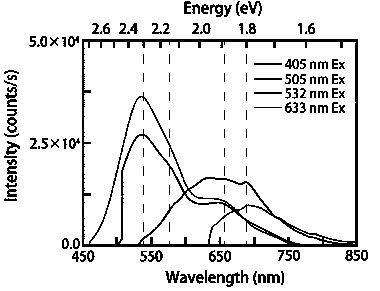
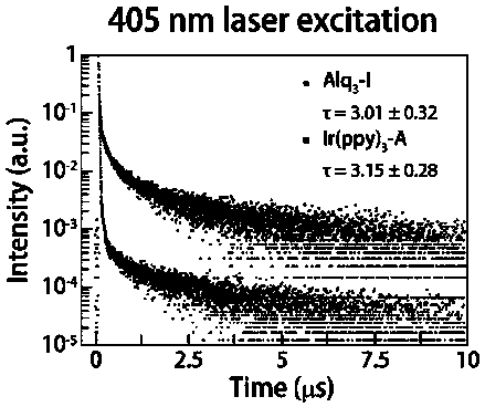
[0054] Product performance test: due to Ir(ppy) 3 Guest material and host material Alq 3 The ligand structure has a similar structure, the ligand of the guest material is phenylpyridine, and the ligand of the host material is hydroxyquinoline; and the atomic radius of the metal complex of the host material and the guest material has a large gap, and the guest material is He...

Embodiment 2

[0056] Raw material: guest material Alq 3 and host material Ir(ppy) 3

[0057] Preparation:

[0058] 1) In an inert environment, the guest material Alq 3 and host material Ir(ppy) 3 Two pieces of metal complex amorphous doped films prepared by co-evaporation are stacked face to face, and then placed on a closed hot stage;

[0059] 2) Heating the stacked metal complex amorphous doped film to 300°C and annealing for 25 minutes;

[0060] 3) Stop heating and cool to room temperature in a nitrogen environment to obtain defect-induced organic crystal materials.

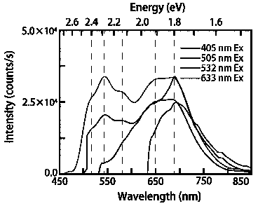
[0061] Product performance test: due to Alq 3 Guest material and host material Ir(ppy) 3 The ligand structure has a similar structure, the ligand of the guest material is hydroxyquinoline, and the ligand of the host material is phenylpyridine; and the atomic radius of the metal complex of the host material and the guest material has a large gap, and the guest material is Light metal Al, the main material is heavy me...


PUM


Abstract

The invention relates to the field of organic semiconductors, and particularly discloses a preparation method of an organic crystalline material, the organic crystalline material and a light-emittingelement. The preparation method of the organic crystalline material comprises the following steps: heating and annealing two oppositely stacked metal complex amorphous doped membranes in an inert environment, and then cooling to room temperature, wherein the host material of the metal complex amorphous doped membranes is a complex of a first metal and a first ligand, and the guest material is a complex of a second metal and a second ligand; moreover, the difference between the metal atomic numbers of the first metal and the second metal is greater than or equal to 10, and the first ligand andthe second ligand are the same or have spatially similar structures. According to the preparation method, the high-concentration doped defect-induced organic crystalline material can be obtained, thephotoluminescence spectrum of the prepared organic crystalline material has triplet state direct excitation and emission characteristics, and the organic crystalline material can be applied to a light-emitting element.

Description

technical field [0001] The invention relates to the field of organic semiconductors, in particular to a preparation method of an organic crystal material, an organic crystal material and a light-emitting element. Background technique [0002] The synthesis and optimization of organic semiconductor materials are mainly based on the synthesis of various types of organic molecules, through the optimization of different ligands and groups, to achieve electron injection and transport capabilities at different energy levels. Molecular energy levels can be classified into singlet and triplet properties based on the electron pairing of the outer electron energy levels. The triplet energy level of organic molecules is often considered to be forbidden, and its role in the electronic transition during the luminescence process and the electron transport process of the device is much lower than that of the singlet energy level. [0003] Introducing defects into crystals is a common meth...

Claims


Application Information

Patent Timeline
IPC IPC(8): C30B29/54C30B1/02C23C14/12C09K11/02C09K11/06H01L51/50H01L51/54
CPCC30B29/54C30B1/023C23C14/12C09K11/02C09K11/06C09K2211/181C09K2211/185C09K2211/186H10K85/30H10K85/324H10K85/342H10K50/00
Inventor 毕海宋小贤王悦霍婵媛
Owner JIHUA LAB
Why Eureka
Try Eureka