

Light-emitting field-effect transistor with dielectric layer/quantum dot/dielectric layer structure and preparation method thereof
A field-effect transistor and quantum dot light-emitting technology, which is applied in the fields of electric solid-state devices, semiconductor/solid-state device manufacturing, circuits, etc., can solve the problems of unfavorable hole injection into the quantum dot light-emitting layer, reducing the light-emitting performance of the device, and deteriorating the light-emitting efficiency of the device. , to achieve the effect of reducing trap density, improving injection efficiency and low cost
- Summary
- Abstract
- Description
- Claims
- Application Information
AI Technical Summary
Problems solved by technology
Method used
Image

Examples
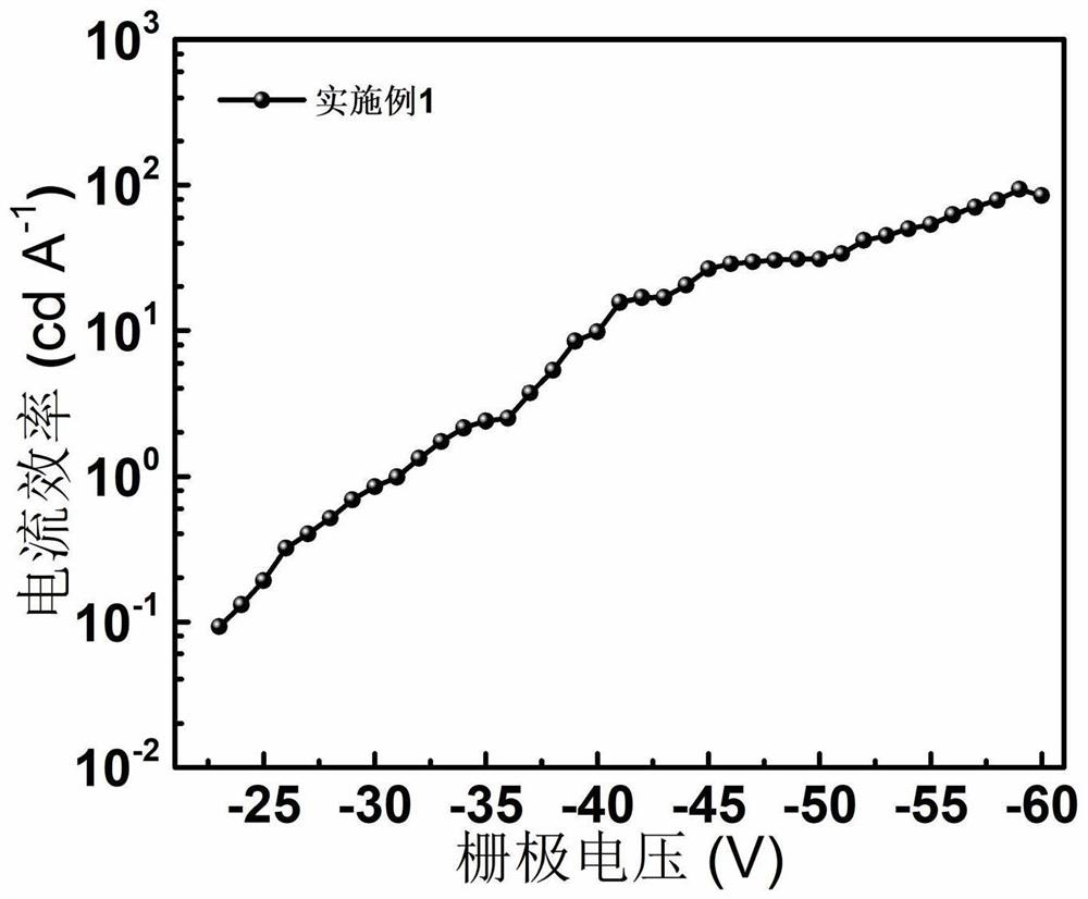
Embodiment 1
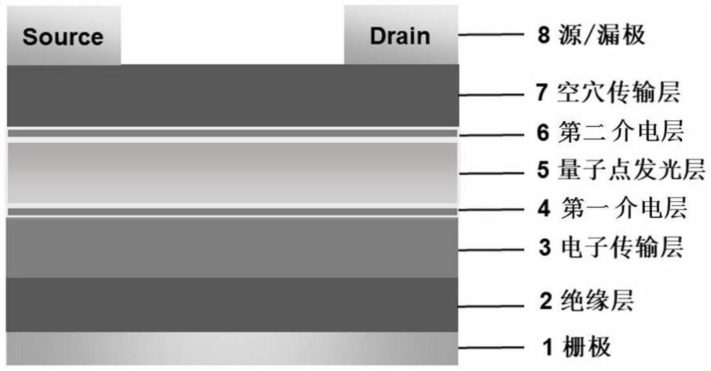
[0035] In this example, see figure 1 , a light-emitting field-effect transistor with a dielectric layer / quantum dot / dielectric layer structure, in which a gate 1, an insulating layer 2, an electron transport layer 3, a first dielectric layer 4, and a quantum dot light-emitting layer are sequentially arranged from bottom to top layer 5, second dielectric layer 6, hole transport layer 7, source / drain 8;
[0036] The thickness of the gate 1 is 150nm, and the gate 1 is made of ITO conductive glass;
[0037] The insulating layer 2 has a thickness of 150nm, and the insulating layer 2 is made of aluminum oxide (Al 2 o 3 )film;
[0038] The electron transport layer 3 has a thickness of 70nm, and the electron transport layer 3 is made of zinc oxide nanoparticles into a zinc oxide film;
[0039] The thickness of the first dielectric layer 4 is 3 nm, and the first dielectric layer 4 adopts a methyl ammonium bromide (MABr) film;
[0040] The quantum dot luminescent layer 5 has a thic...
Embodiment 2
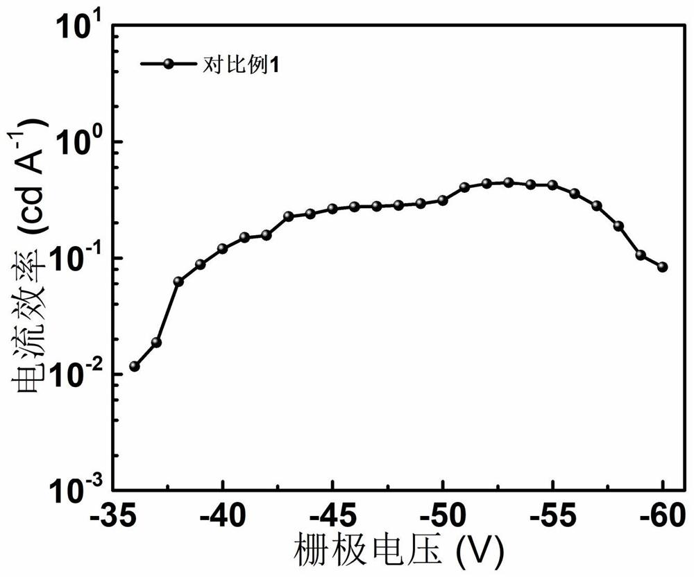
[0065] This embodiment is basically the same as Embodiment 1, especially in that:
[0066] In this example, see figure 1 , a light-emitting field-effect transistor with a dielectric layer / quantum dot / dielectric layer structure, in which a gate 1, an insulating layer 2, an electron transport layer 3, a first dielectric layer 4, and a quantum dot light-emitting layer are sequentially arranged from bottom to top layer 5, second dielectric layer 6, hole transport layer 7, source / drain 8;
[0067] The thickness of the gate 1 is 100nm, and the gate 1 is made of ITO conductive glass;
[0068] The insulating layer 2 has a thickness of 140nm, and the insulating layer 2 is made of aluminum oxide (Al 2 o 3 )film;
[0069] The electron transport layer 3 has a thickness of 60nm, and the electron transport layer 3 is made of zinc oxide nanoparticles into a zinc oxide film;
[0070] The thickness of the first dielectric layer 4 is 1 nm, and the first dielectric layer 4 adopts a methyl a...
PUM
| Property | Measurement | Unit |
|---|---|---|
| Thickness | aaaaa | aaaaa |
| Thickness | aaaaa | aaaaa |
| Thickness | aaaaa | aaaaa |
Abstract
Description
Claims
Application Information