Magnetic field sensor based on organic field effect transistor and preparation method thereof
A magnetic field sensor and effect tube technology, which is applied in the direction of the size/direction of the magnetic field, semiconductor/solid-state device manufacturing, and magnetic field measurement using electromagnetic devices. It can solve the problems of large size, non-portable application range, and complex structure. Good performance, uniform and controllable size, widening the application range
- Summary
- Abstract
- Description
- Claims
- Application Information
AI Technical Summary
Problems solved by technology
Method used
Image


Examples
Embodiment 1
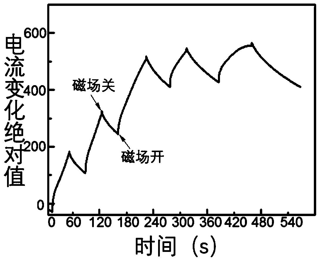
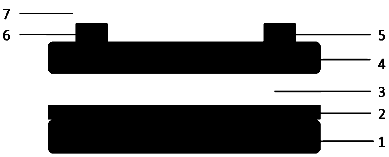
[0039] like Figure 1-2As shown, a magnetic field sensor based on an organic field effect transistor, the magnetic field sensor includes a substrate 1, a gate electrode 2, a dielectric layer 3, an organic semiconductor layer 4, a source electrode 5, a drain electrode 6 and a package from bottom to top. Layer 7, the organic semiconductor layer 4 includes a mixed material of magnetic nanomaterials and organic semiconductor materials, wherein the bottom gate top contact structure, the gate electrode 2, the source electrode 5 and the drain electrode 6 are all silver nanowires, and the dielectric layer 3 is made of polystyrene with a thickness of 500nm, the semiconductor layer 4 is formed by mixing 3-hexylthiophene and iron nanoparticles (0.1 wt%) with a thickness of 50nm, and the shellac encapsulation layer 7 has a thickness of 300nm. A field effect transistor magnetic field sensor with high sensitivity and high stability can be realized by using the structure.
[0040] A method ...
Embodiment 2
[0049] like figure 1 As shown, a magnetic field sensor based on an organic field effect transistor, the magnetic field sensor includes a substrate 1, a gate electrode 2, a dielectric layer 3, an organic semiconductor layer 4, a source electrode 5, a drain electrode 6 and a package from bottom to top. Layer 7, the organic semiconductor layer 4 includes a mixed material of magnetic nanomaterials and organic semiconductor materials, wherein the bottom gate top contact structure, the gate electrode 2, the source electrode 5 and the drain electrode 6 are all gold nanowires, and the dielectric layer 3 is polymethyl methacrylate, the thickness is 300nm, the semiconductor layer 4 is formed by mixing Tips-pentacene and nickel nanoparticles (0.5wt%), the thickness is 70nm, and the shellac encapsulation layer 7 is 200nm in thickness. A field effect transistor magnetic field sensor with high sensitivity and high stability can be realized by using the structure.
[0050] A method for prep...
Embodiment 3
[0058] like figure 1 As shown, a magnetic field sensor based on an organic field effect transistor, the magnetic field sensor includes a substrate 1, a gate electrode 2, a dielectric layer 3, an organic semiconductor layer 4, a source electrode 5, a drain electrode 6 and a package from bottom to top. Layer 7, the organic semiconductor layer 4 includes a mixed material of magnetic nanomaterials and organic semiconductor materials, wherein the bottom gate top contact structure, the gate electrode 2, the source electrode 5 and the drain electrode 6 are all indium nanowires, and the dielectric layer 3 adopts polyvinyl alcohol, the thickness is 300nm, the semiconductor layer 4 is the polyisoprene derivative containing siloxane and cobalt nanoparticle (content is 1wt%) mixed composition, and the thickness is 60nm, and the shellac encapsulation layer 7 thickness is 250nm. A field effect transistor magnetic field sensor with high sensitivity and high stability can be realized by usin...
PUM
| Property | Measurement | Unit |
|---|---|---|
| thickness | aaaaa | aaaaa |
| thickness | aaaaa | aaaaa |
| thickness | aaaaa | aaaaa |
Abstract
Description
Claims
Application Information
 - R&D
- Intellectual Property
- Life Sciences
- Materials
- Tech Scout
- Unparalleled Data Quality
- Higher Quality Content
- 60% Fewer Hallucinations
Browse by: Latest US Patents, China's latest patents, Technical Efficacy Thesaurus, Application Domain, Technology Topic, Popular Technical Reports.
© 2025 PatSnap. All rights reserved.Legal|Privacy policy|Modern Slavery Act Transparency Statement|Sitemap|About US| Contact US: help@patsnap.com