An infrared detector based on an organic field effect tube and its preparation method
An infrared detector and organic field technology, which is applied in the fields of organic semiconductor devices, semiconductor/solid-state device manufacturing, electric solid-state devices, etc., to achieve the effect of improving detection performance, improving response, and simple extraction process
- Summary
- Abstract
- Description
- Claims
- Application Information
AI Technical Summary
Problems solved by technology
Method used
Image

Examples
Embodiment 1
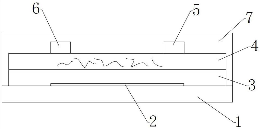
[0041] Such as figure 1 The bottom-gate top-contact structure is shown, and the material and thickness of each layer are as follows: the gate electrode, source electrode and drain electrode are all silver nanowires; the dielectric layer is made of silk fibroin with a thickness of 200nm; the organic semiconductor layer is made of carbon nanowires. The pipe is formed by mixing bamboo fibers (bamboo fiber mass fraction is 10%), and the thickness is 50nm; the shellac encapsulation layer has a thickness of 300nm. A field effect transistor infrared detector with high sensitivity and high stability can be realized by using the structure.
[0042] The preparation method of the present embodiment is as follows:
[0043] ① Clean the substrate with detergent, acetone solution, deionized water and isopropanol solution, and dry it with nitrogen after cleaning;
[0044] ② Prepare a 30nm thick silver nano wire grid electrode on the surface of the substrate;
[0045] ③The silk fibroin solu...
Embodiment 2
[0050] Such as figure 1 The bottom-gate top-contact structure is shown, and the material and thickness of each layer are as follows: the gate electrode, source electrode and drain electrode are all gold nanowires; the dielectric layer is made of silk fibroin with a thickness of 500nm; the organic semiconductor layer is 3- Hexylthiophene is mixed with bamboo fiber (the mass fraction of bamboo fiber is 5%), and the thickness is 30nm; the shellac encapsulation layer has a thickness of 200nm. A field effect transistor infrared detector with high sensitivity and high stability can be realized by using the structure.
[0051] The preparation method of the present embodiment is as follows:
[0052] ① Clean the substrate with detergent, acetone solution, deionized water and isopropanol solution, and dry it with nitrogen after cleaning;
[0053] ② Prepare a 30nm thick gold nano wire grid electrode on the surface of the substrate;
[0054] ③The silk fibroin solution with a concentrat...
Embodiment 3
[0059] Such as figure 1 The bottom-gate top-contact structure is shown, and the material and thickness of each layer are as follows: the gate electrode, source electrode and drain electrode are all iron nanowires; the dielectric layer is silk fibroin with a thickness of 600nm; the organic semiconductor layer is 6, 13-bis(triisopropylsilylethynyl) pentacene is mixed with bamboo fiber (the mass fraction of bamboo fiber is 8%), the thickness is 40nm, and the shellac encapsulation layer has a thickness of 200nm. A field effect transistor infrared detector with high sensitivity and high stability can be realized by using the structure.
[0060] The preparation method of the present embodiment is as follows:
[0061] ① Clean the substrate with detergent, acetone solution, deionized water and isopropanol solution, and dry it with nitrogen after cleaning;
[0062] ② Prepare a 30nm thick iron nano wire grid electrode on the surface of the substrate;
[0063] ③The silk fibroin soluti...
PUM
| Property | Measurement | Unit |
|---|---|---|
| thickness | aaaaa | aaaaa |
| thickness | aaaaa | aaaaa |
| thickness | aaaaa | aaaaa |
Abstract
Description
Claims
Application Information
 - R&D
- Intellectual Property
- Life Sciences
- Materials
- Tech Scout
- Unparalleled Data Quality
- Higher Quality Content
- 60% Fewer Hallucinations
Browse by: Latest US Patents, China's latest patents, Technical Efficacy Thesaurus, Application Domain, Technology Topic, Popular Technical Reports.
© 2025 PatSnap. All rights reserved.Legal|Privacy policy|Modern Slavery Act Transparency Statement|Sitemap|About US| Contact US: help@patsnap.com