GaN-based PN diode and preparation method thereof

A diode, p-type technology, applied in the field of GaN-based PN diodes and their preparation, can solve problems such as unfavorable device output current, increased material carrier scattering probability, etc., to maintain mobility and increase reverse breakdown voltage. , the effect of improving the doping efficiency

Pending Publication Date: 2020-05-19
SHENZHEN INST OF WIDE BANDGAP SEMICON
View PDF9 Cites 5 Cited by
  • Summary
  • Abstract
  • Description
  • Claims
  • Application Information

AI Technical Summary

Problems solved by technology

However, the existing technical solutions not only have great difficulties in obtaining a P-type region with high carrier concentration, but also increase the carrier concentration by increasi

Method used


Image

  • GaN-based PN diode and preparation method thereof
  • GaN-based PN diode and preparation method thereof
  • GaN-based PN diode and preparation method thereof

Examples


Embodiment Construction

[0023] In order to make the object, technical solution and advantages of the present invention clearer, the present invention will be further described in detail below in conjunction with specific embodiments and with reference to the accompanying drawings.

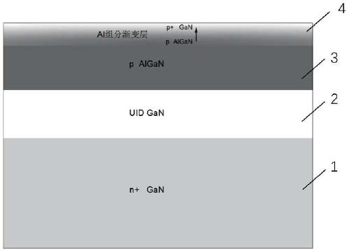
[0024] Embodiment This embodiment provides a vertical GaN-based PN diode and its preparation method

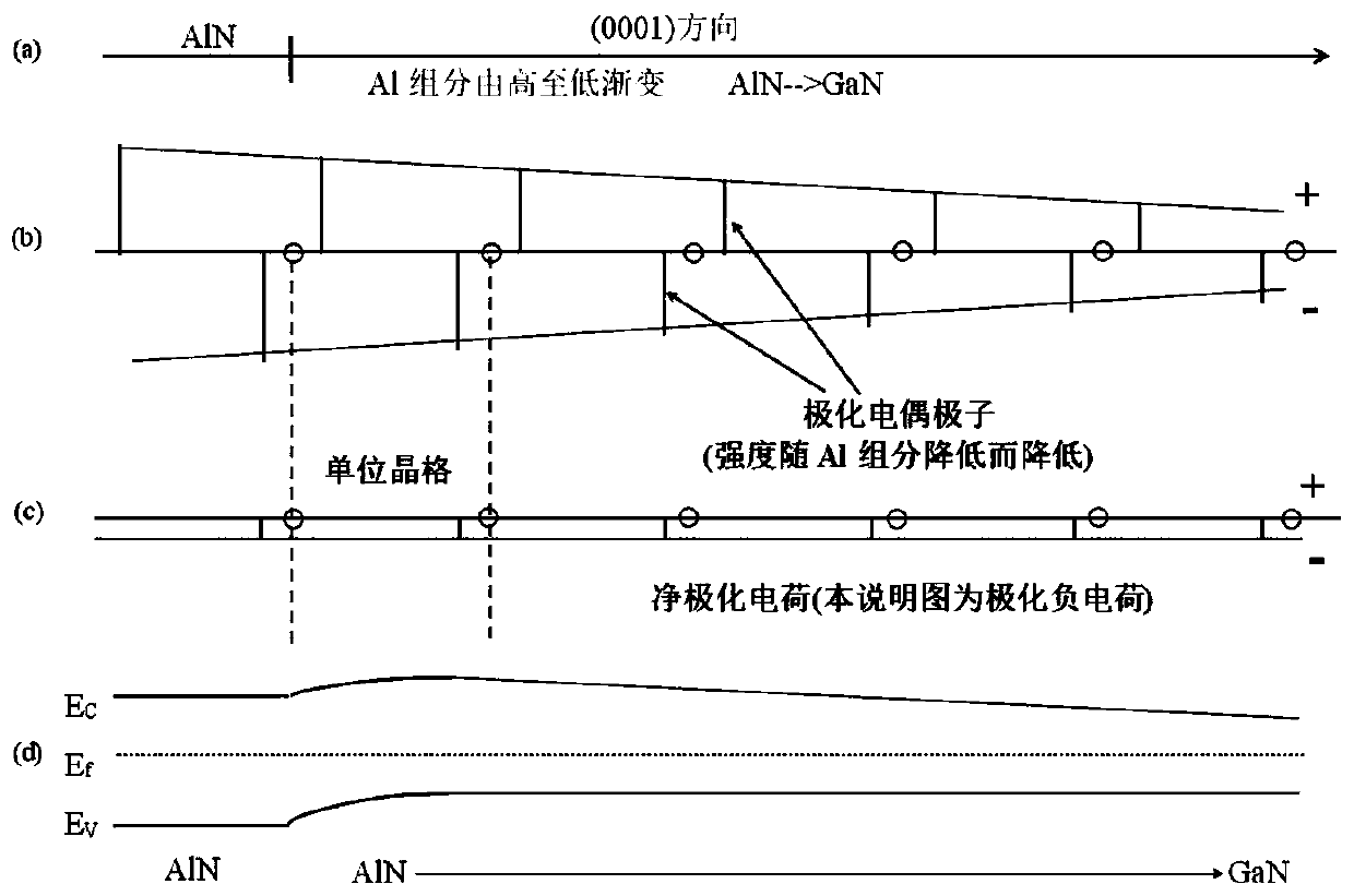
[0025] Such as figure 1 As shown, the GaN-based PN diode structure in this example is a highly doped n+-type GaN substrate 1 with a thickness of 9 μm, a non-doped GaN layer 2, a p-type AlGaN layer 3 with a thickness of 450 nm, and a thickness of 9 μm from bottom to top. 50nm p-type AlGaN graded structure 4, where 0≤x≤0.4, and the electron concentration of n+-type GaN substrate 1 is 10 18 cm -3 ~10 20 cm -3 , the electron concentration of the undoped GaN layer 2 is 10 15 cm -3 ~10 17 cm -3 , the hole concentration of the p-type AlGaN layer 3 is 10 17 cm -3 ~10 18 cm -3 , the Al composition in the p-type AlGaN l...


PUM

PropertyMeasurementUnit
Thicknessaaaaaaaaaa
Thicknessaaaaaaaaaa
Electron concentrationaaaaaaaaaa

Abstract

The invention provides a GaN-based PN diode and a preparation method thereof. The GaN-based PN diode sequentially comprises a highly-doped n+ type GaN substrate 1, a non-doped GaN layer 2, a p type AlGaN layer 3 and a p type AlGaN gradient structure 4 from bottom to top, wherein the molar content of an Al component in the p type AlGaN layer 3 is 0.2-0.4 of the sum of the Al component and a Ga component; and in the p-type AlGaN gradual change structure 4, the Al component is gradually reduced from bottom to top, and the reduction gradient is gradually increased until the top of the p-type AlGaNgradual change structure is a GaN layer. Because of the polarization effect of the gradient structure, fixed negative polarization charges are introduced to induce generation of free holes, the doping efficiency is improved, the carrier scattering probability can be reduced and the carrier mobility is improved while high hole concentration is realized at relatively low doping concentration, so that the PN diode can obtain high-quality P-type ohmic contact and higher output current more easily.

Description

technical field [0001] The invention belongs to the field of semiconductor devices, in particular to a GaN-based PN diode and a preparation method thereof. Background technique [0002] As a third-generation semiconductor material, Gallium Nitride has the characteristics of wide bandgap, high breakdown field strength, good heat dissipation, and spontaneous polarization. At the same time, it has stable physical and chemical properties, corrosion resistance, and radiation resistance. It is regarded as It is the material of choice for the next generation of electronic devices working in complex environments such as high voltage and high frequency. Due to the material properties of high withstand voltage and high electron mobility, gallium nitride is widely used in power electronic devices such as PN diodes. However, in the process of GaN PN junction epitaxial growth, the P-type region is often formed by introducing the doping element Mg in the epitaxial growth, and then releas...

Claims


Application Information

Patent Timeline
IPC IPC(8): H01L29/868H01L29/20H01L29/207H01L21/329
CPCH01L29/2003H01L29/207H01L29/868H01L29/66204
Inventor 刘新科胡聪高博
Owner SHENZHEN INST OF WIDE BANDGAP SEMICON
Why Eureka
Try Eureka