LED Bin dividing method and application product thereof

A product and standard technology, applied in the field of LED product application, can solve problems such as random selection of color coordinate range, insufficient research, different color saturation or color purity, etc., to achieve simple and convenient implementation, excellent light and color consistency, Good color consistency

Inactive Publication Date: 2020-05-22
轻工业部南京电光源材料科学研究所
View PDF6 Cites 6 Cited by
  • Summary
  • Abstract
  • Description
  • Claims
  • Application Information

AI Technical Summary

Problems solved by technology

[0004] For display LED products, basically all LED wafer or package manufacturers on the market use wavelength, brightness and voltage as binning conditions, such as figure 1 As shown, one reason is that there are differences due to different application fields; another reason is that the research on light chromaticity in the display industry is not thorough enough; in addition, due to the huge demand for display products, existing methods can reduce the proportion of out-of-range and improve Product yield
[0005] In view of the above reasons, from theoretical analysis, there is a certain correspondence between wavelength and chromaticity, such as figure 2 As shown, although the dominant wavelength parameter in the existing display LED binning method has a certain limit on the chromaticity, but because the products with the same dominant wavelength have different color saturation or color purity, there is still a certain color difference in the same Bin product. Deviation problem, which can be compared intuitively in the CIE color coordinate map, such as image 3 As shown, this is also the blurred screen phenomenon that we often see after the LED display is assembled, ...

Method used


Image

  • LED Bin dividing method and application product thereof
  • LED Bin dividing method and application product thereof
  • LED Bin dividing method and application product thereof

Examples


Embodiment 1

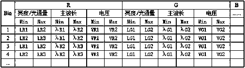
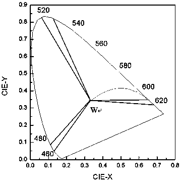
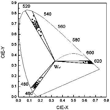
[0045] Such as Figure 4 As shown, it is used to illustrate a kind of LED binning method involved in the present invention and a flow diagram of its application products. In this embodiment, the bin objects are selected as LED full-color packaging products, and the specific models are surface mount 1010 / 1515 / 2727 / 3535, etc., and the RGB main wavelength interval span is defined as 4nm (maximum value-minimum value), and the brightness interval span is 1:1.2 (minimum value: maximum value / minimum value), the voltage interval span is 0.6V (maximum value-minimum value), and the color purity interval span is 15% (maximum value-minimum value).

[0046] Randomly select a certain amount of packaged samples to be binned, and the number of samples to be tested shall not be less than 10% of the total product. Test the main wavelength, brightness, voltage, and color coordinates of the product under the RGB binning current (20-20-20mA) respectively, and Do statistical analysis on the first ...

Embodiment 2

[0062] Referring to Example 1, in addition to those described in Example 1, the parameters in the LED bin standard may or may not include parameters such as leakage current, power, peak wavelength, half-wave width, color rendering index, and color temperature.


PUM


Abstract

The invention discloses an LED Bin dividing method and an application product thereof. The LED Bin dividing method and an application product thereof are characterized in that LED Bin dividing parameters included in the method at least comprise brightness or luminous fluxes, voltage and chromaticity coordinates of wafers in LEDs, according to actual distribution conditions of the LED parameters under preset conditions, the parameters are divided into different section ranges, and the parameters in the sections are arranged and combined together to form a final Bin dividing standard. The Bin dividing condition or range of the Bin dividing parameters is reasonably and scientifically defined, scientific definition of optics, electricity and chromaticity is included, products with similar parameters are concentrated in a same Bin, LED products with Bin divided through the method are assembled together, color consistency of end application products can be greatly improved, and color difference or color deviation problems of a same batch of products can be solved.

Description

technical field [0001] The invention belongs to the application field of LED products, and in particular relates to an LED binning method and the application of LED products binned by the method to terminal products. Background technique [0002] Compared with other light-emitting products, LED products have the advantages of excellent energy saving and environmental protection, long life, low cost, etc., so they have been extensively studied and their technological level has developed rapidly. [0003] Before the existing LED products are assembled into final products, in order to eliminate color differences, they must be binned or screened, so that products with similar parameters are divided into one Bin for assembly. The current mainstream binning method is to test and sort the parameters of the LED through a certain interval range under a certain driving current, mainly including the main wavelength, brightness, color temperature, luminous flux, voltage, color coordinat...

Claims


Application Information

Patent Timeline
IPC IPC(8): B07C5/342B07C5/344B07C5/36H01L33/00G01R31/26G01R31/44
CPCB07C5/342B07C5/344B07C5/362G01R31/2601G01R31/44H01L33/0095
Inventor 刘晓锋蒋腾童嘉俊尤宇财卓宁泽刘光熙郭健王海波
Owner 轻工业部南京电光源材料科学研究所
Why Eureka
Try Eureka