Near-field microwave measurement system based on impedance measurement

A microwave measurement and impedance measurement technology, applied in the measurement of electrical variables, measurement devices, dielectric properties measurement and other directions, can solve the problems of slow test speed, no measurement, spatial resolution as low as 0.1μm, etc., to simplify motion control system, improve the accuracy of position control, and reduce the cost of implementation

Pending Publication Date: 2020-05-22
张洮 +1
View PDF17 Cites 3 Cited by
  • Summary
  • Abstract
  • Description
  • Claims
  • Application Information

AI Technical Summary

Problems solved by technology

The use of low-frequency phase-locked amplification in the detection system has the following disadvantages: a part of the near-field electromagnetic interaction information contained in the reflected microwave signal of the measured object may be lost in the signal demodulation link; in order to stabilize the signal, it is usually necessary to set a low-frequency phase-locked amplifier of more than 10 milliseconds The time constant of the amplified filter is slow to test; the low-frequency lock-in amplifier is a relatively expensive instrument, which is difficult to realize with a single integrated circuit, and it is difficult to miniaturize the system; the modulation of the incident microwave signal below 100KHz increases the realization of the near-field microwave measurement system unnecessary complexity
Using the resonant frequency offset feedback of the microwave resonator to control the absolute position of the probe from the measured object has the following disadvantages: it can only be used in a narrow frequency range near the microwave resonant frequency, and when the test frequency is not near the resonant frequency, This control strategy is ineffective; measuring resonator frequency offset requires frequency modulation and a low frequency lock-in amplifier
The surface of the measured object is irradiated with X-rays to construct an image similar to computed tomography (CT), and the spatial resolution of the X-ray microanalysis system is as low as 0.1 μm
These methods are mainly used to measure the geometric characteristics below the surface of the measured object, and do not have the ability to measure the parameters of the material properties below the surface

Method used


Image

  • Near-field microwave measurement system based on impedance measurement
  • Near-field microwave measurement system based on impedance measurement

Examples


Embodiment 1

[0039] Factors such as the chemical composition of the liquid, ion concentration, and temperature can change the dielectric parameters of the liquid. By directly quantitatively measuring the dielectric parameters of liquids, parameters such as chemical composition, ion concentration and temperature can be measured without contact.

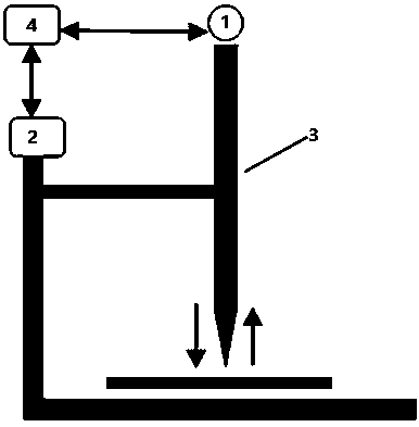
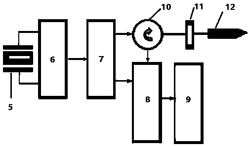
[0040] In an exemplary embodiment of the present invention, a near-field microwave measurement system for dielectric parameters of a liquid object to be measured is provided, with an operating frequency range of 20 GHz to 25 GHz. The system includes: a microwave network analysis system 1 , a position device 2 , a near-field microwave impedance sensor 3 and a data processing system 4 . The microwave network analysis system 1 is configured to generate a microwave signal and input it to the near-field microwave impedance sensor 3 to determine the complex impedance. The position device 2 is configured to fix the near-field microwave impedance sensor 3...

Embodiment 2

[0051] In the production or quality control of layered products such as glass, semiconductor wafers or PCB boards, high spatial resolution material parameters and surface morphology detection of layered objects can be used to feedback control process parameters and improve yield. Differences in material properties below the surface of the material target area alter the dielectric properties of the material target area. These tests should have the following characteristics: non-contact, non-destructive, fast, and high sensitivity. To reduce the size of the sensor probe, the near-field microwave measurement system uses the electromagnetic interaction between the sensor probe and the measured object in the near field, which can break through the diffraction limit and achieve a spatial resolution of less than λ / 2.

[0052] In an exemplary embodiment of the present invention, a near-field microwave measurement system for material parameters and surface topography of a layered objec...


PUM


Abstract

The invention provides a near-field microwave measurement system based on impedance measurement. The near-field microwave measurement system comprises a microwave network analysis system, a position device, a near-field microwave impedance sensor and a data processing system. A complex impedance for determining of a near-field microwave impedance sensor is provided; the absolute position for controlling a probe to a measured object is fed back by probe impedance; and material property parameters or surface topography of the measured object are obtained from the impedance and position parameters of the probe. The system can be used to solve the technical problems that substance properties or surface topography of a sample cannot be quantitatively detected by a high-resolution optical testing technology; that a traditional technology for quantitatively testing dielectric parameters in a microwave frequency spectrum is difficult to use in a microscopic system; and that a traditional near-field microwave measurement system needs to modulate and demodulate incident microwave signals, a low-frequency phase-locked loop with the frequency below 100 KHz is used, influence of substance property parameters and the position of the probe relative to the measured object on microwave signals reflected by the measured object is difficult to decouple, the absolute position of the probe away from the measured object cannot be reliably controlled, and the low-frequency phase-locked loop can only be used for narrow-frequency-band measurement.

Description

technical field [0001] The invention relates to a dielectric parameter and surface topography measurement technology of a measured object at a microwave frequency, in particular to a near-field microwave measurement system based on impedance measurement, which belongs to the field of microwave measurement technology. Background technique [0002] Microwave refers to the electromagnetic spectrum with a frequency from 300MHz to 300GHz. Limited by the Abelian diffraction phenomenon, the spatial resolution of far-field imaging can generally only reach the millimeter level (~λ / 2, where λ is the wavelength). Using the electromagnetic interaction between the sensor probe and the measured object in the near field, the near-field microwave measurement system can break through the diffraction limit and achieve a spatial resolution smaller than microns. [0003] At present, most near-field microwave measurement systems include a low-frequency lock-in amplification link below 100KHz: fr...

Claims


Application Information

Patent Timeline
Patent Type & Authority Applications(China)
IPC IPC(8): G01N22/00G01R27/26G01B15/04
CPCG01N22/00G01R27/2617G01B15/04
Inventor 张洮
Owner 张洮
Why Eureka
Try Eureka