Photoelectric calculation unit, photoelectric calculation array and photoelectric calculation method
A computing unit and light-emitting unit technology, applied in optical computing equipment, computing, computers, etc., can solve the problems of unguaranteed device yield and uniformity, and unsupported RRAM.
- Summary
- Abstract
- Description
- Claims
- Application Information
AI Technical Summary
Problems solved by technology
Method used
Image
Examples
no. 1 example
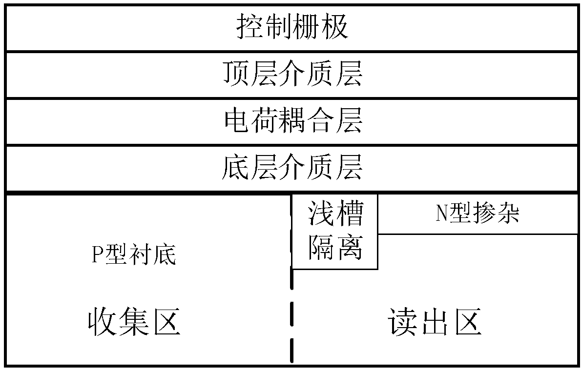
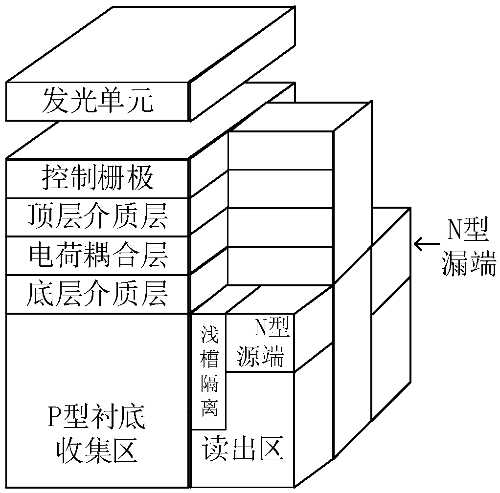
[0058] Reference Figure 2 to 5 The optoelectronic calculation unit according to the first embodiment of the present invention is described.
[0059] Such as figure 2 with image 3 As shown in the front view and the three-dimensional view of the optoelectronic computing unit, there is a P-type semiconductor substrate as the photo-generated carrier collection area and the readout area, which is divided into a left collection area and a right readout area, wherein the The collection area on the left is used to apply a pulse with a voltage range of negative voltage on the substrate, or a pulse with a voltage range of positive voltage on the control gate, so that a depletion layer for photoelectron collection is generated in the substrate of the collection area , And read the collected photoelectron quantity through the right readout area as the input quantity of the light input end. The right read area includes shallow trench isolation, N-type drain and N-type source. The shallow ...
no. 2 example
[0106] Reference Figure 6 to 8 The photoelectric calculation unit according to the second embodiment of the present invention is described.
[0107] Such as Image 6 with Figure 7 As shown in the front view and three-dimensional view of the optoelectronic computing unit, there is an N-type semiconductor substrate as a photo-generated carrier collection and readout area, which is divided into a left collection area and a right readout area. The left readout area is used to apply a pulse with a voltage range of positive voltage on the substrate, or apply a pulse with a voltage range of negative voltage on the control gate, so that light holes are generated in the substrate of the collection area The depletion layer is collected, and the collected photo-hole charges are read out through the right readout area; the right readout area includes shallow trench isolation, P-type drain and P-type source. The shallow trench isolation is located between the collection area and the readout...
no. 3 example
[0117] Reference Figure 9 to 12 The photoelectric calculation unit according to the third embodiment of the present invention is described.
[0118] Such as Picture 9 with Picture 10 As shown in the front view and the three-dimensional view of the photoelectric computing unit, there is a P-type semiconductor substrate as the photo-generated carrier collection and readout area, which can undertake the work of photosensitive and readout at the same time, including an N-type drain and An N-type source terminal. The N-type source terminal is located on the side close to the bottom dielectric layer in the readout area and is formed by doping by ion implantation. The N-type drain terminal is located on the other side of the semiconductor substrate close to the bottom dielectric layer opposite to the N-type source terminal, and is also formed by doping by ion implantation. During light exposure, a pulse with a voltage range of negative voltage is applied to the P-type semiconductor ...
PUM
 Abstract
Description
Claims
Application Information


