
A method for preparing c-axis preferred orientation aluminum nitride polycrystalline film by magnetron sputtering and aluminum nitride polycrystalline film

A magnetron sputtering and preferred orientation technology, applied in chemical instruments and methods, sputtering coating, polycrystalline material growth and other directions, can solve the problem of low kinetic energy, etc. Coupling coefficient, high crystallinity effect

Active Publication Date: 2022-03-18
河南科之诚第三代半导体碳基芯片有限公司 +1
View PDF3 Cites 0 Cited by
  • Summary
  • Abstract
  • Description
  • Claims
  • Application Information

AI Technical Summary

Problems solved by technology

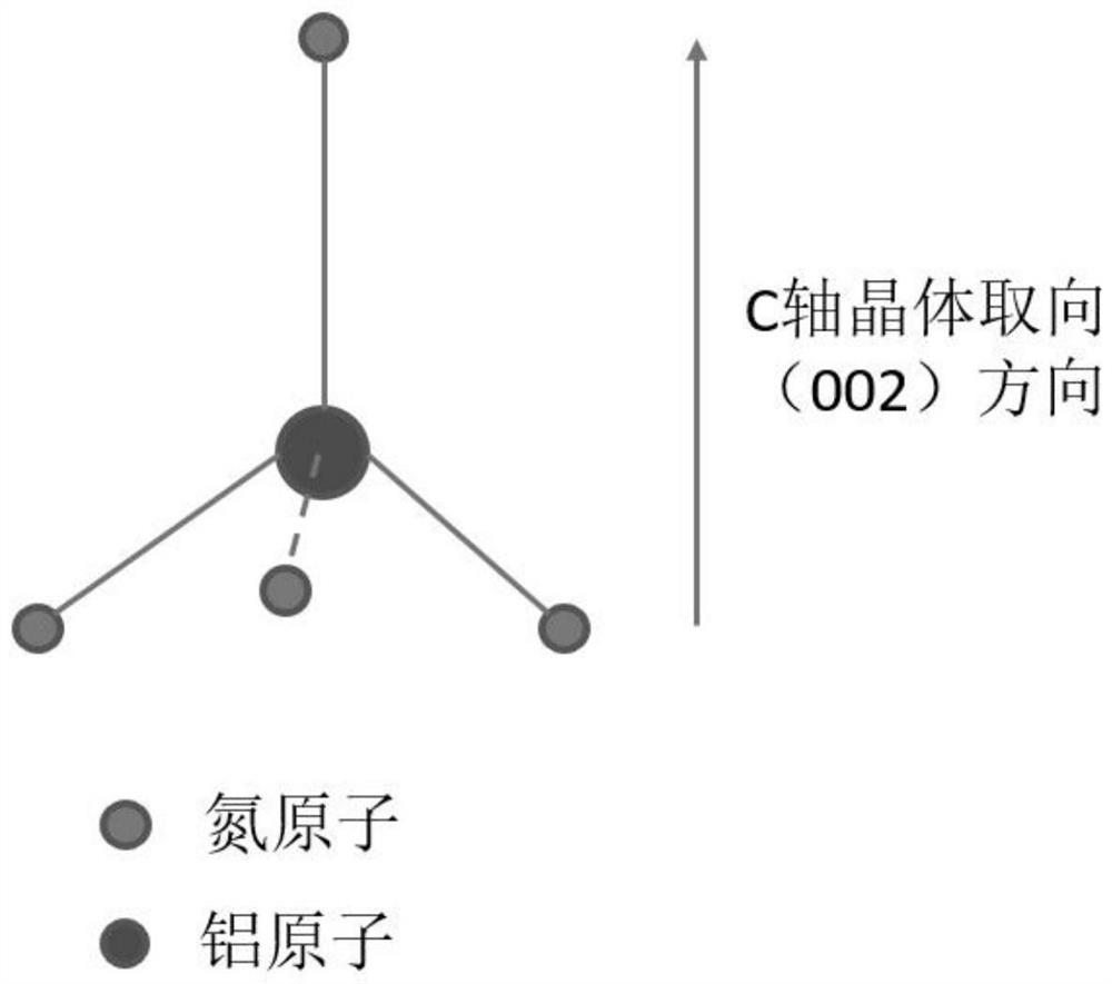
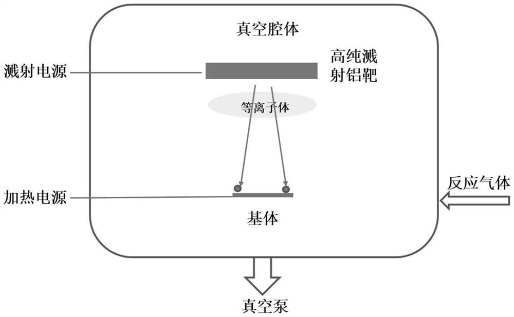
[0005] Although the traditional magnetron sputtering process can prepare AlN thin films, the horizontal movement energy of the sputtered particles reaching the substrate surface is low, and it is difficult to form C-axis oriented AlN thin films.

Method used


Image

  • A method for preparing c-axis preferred orientation aluminum nitride polycrystalline film by magnetron sputtering and aluminum nitride polycrystalline film
  • A method for preparing c-axis preferred orientation aluminum nitride polycrystalline film by magnetron sputtering and aluminum nitride polycrystalline film
  • A method for preparing c-axis preferred orientation aluminum nitride polycrystalline film by magnetron sputtering and aluminum nitride polycrystalline film

Examples


Embodiment 1

[0051] Magnetron sputtering to prepare C-axis preferred orientation aluminum nitride polycrystalline film, the steps are as follows:

[0052] The semiconductor material substrate is on a 2-inch silicon substrate, the silicon substrate is P-type doped, the thickness is 0.5mm, and the surface polishing roughness is less than 8nm; the substrate is placed horizontally on the sample stage in the vacuum chamber, and the sample stage can rotate around the center. The platform controls the substrate temperature to 300°C;

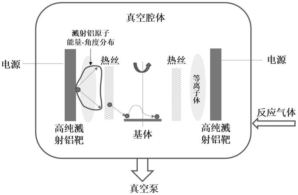
[0053] 4 columnar high-purity sputtering aluminum targets are vertically and evenly distributed around the sample stage (the normal direction of the silicon substrate surface is perpendicular to the normal direction of the surface of the high-purity sputtering aluminum target), and the diameter of the sputtering aluminum target is 80mm, which is higher than the surface of the substrate 200mm, the horizontal distance between the surface of the sputtering target and t...

Embodiment 2

[0060] Magnetron sputtering to prepare C-axis preferred orientation aluminum nitride polycrystalline film, the steps are as follows:

[0061] The semiconductor material substrate is on a 2-inch silicon substrate, the silicon substrate is P-type doped, the thickness is 0.5mm, and the surface polishing roughness is less than 8nm; the substrate is placed horizontally on the sample stage in the vacuum chamber, and the sample stage can rotate around the center. The platform controls the substrate temperature to 300°C;

[0062] A single annular high-purity sputtering aluminum target surrounds the sample stage (the normal direction of the surface of the silicon substrate is perpendicular to the normal direction of the surface of the high-purity sputtering aluminum target), the inner diameter of the sputtering aluminum target is 250mm, the wall thickness is 15mm, and it is higher than the substrate The surface is 200mm, and the horizontal distance between the surface of the sputtering...


PUM

PropertyMeasurementUnit
surface roughnessaaaaaaaaaa
thicknessaaaaaaaaaa
diameteraaaaaaaaaa

Abstract

The invention provides a method for preparing a C-axis preferred orientation aluminum nitride polycrystalline film by magnetron sputtering and the aluminum nitride polycrystalline film, and relates to the technical field of film material preparation. In the present invention, the semiconductor material substrate and the high-purity sputtering aluminum target are relatively vertically placed, which can greatly increase the energy of migrating and moving parallel to the surface of the substrate after the sputtered aluminum atomic group reaches the substrate, and is conducive to the growth of the C-axis preferred orientation of the aluminum nitride film. Improve the piezoelectric response and electromechanical coupling coefficient of the film; the invention arranges a hot wire near the semiconductor material substrate, and the high-temperature radiation generated by the hot wire performs rapid heat treatment on the aluminum nitride film, which can improve the crystallization degree of the film. Therefore, the method provided by the present invention can realize the growth of C-axis preferred orientation aluminum nitride film by using magnetron sputtering technology at a lower temperature, and the obtained aluminum nitride film has high crystallinity, high piezoelectric response coefficient and electromechanical coupling The coefficient can be used as a chip material in surface acoustic wave devices or bulk acoustic wave devices.

Description

technical field [0001] The invention relates to the technical field of film material preparation, in particular to a method for preparing a C-axis preferred orientation aluminum nitride polycrystalline film by magnetron sputtering and the aluminum nitride polycrystalline film. Background technique [0002] Surface acoustic wave (SAW) and bulk acoustic wave (BAW) devices can be used in various radio frequency devices, resonators, and sensors. Piezoelectric film, as the substrate for acoustic wave excitation and transmission, is the core chip material of the device. The piezoelectric response coefficient of the material determines the overall performance of the device, which is restricted by the type of material and the crystallographic orientation of the material. For polycrystalline thin films, the film material with preferred orientation is prepared so that the specific crystal direction of all crystal grains is perpendicular to the surface of the substrate, so that the fi...

Claims


Application Information

Patent Timeline
Patent Type & Authority Patents(China)
IPC IPC(8): C23C14/35C23C14/06C23C14/50C30B28/12C30B29/38C30B29/64
CPCC23C14/35C23C14/0641C23C14/505C23C14/0036C30B28/12C30B29/38C30B29/64
Inventor 谢波玮苏广辉张建永丁发柱古宏伟商红静黄大兴李太广邹琪
Owner 河南科之诚第三代半导体碳基芯片有限公司
Learn More