Solar silicon wafer, solar cell, solar cell module and manufacturing method thereof
A technology of solar cells and solar silicon wafers, applied in the field of solar photovoltaic, can solve the problems of incapable of maximizing the use of the component area and reducing the overall efficiency of the components, so as to increase the photoelectric conversion area, improve the photoelectric conversion efficiency, and increase the effective area Effect
- Summary
- Abstract
- Description
- Claims
- Application Information
AI Technical Summary
Problems solved by technology
Method used
Image


Examples
Embodiment 1
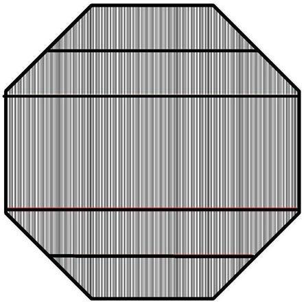
[0041] The present disclosure provides a solar silicon wafer, such as figure 1 As shown, the solar silicon wafer is a regular octagon. The diameter of the circumscribed circle of the regular octagon is 150 mm to 300 mm.
[0042] In an example of the present disclosure, the regular octagonal silicon wafer is cut into octagonal pillars along the octagonal axis inscribed in the cross-section of the cylindrical silicon rod, and then sliced. Specifically, crystal silicon rods are made into regular octagonal solar silicon wafers through processes such as crystal growth, square extraction, end face processing, and diamond wire slicing.
[0043] The silicon chip in this disclosure is a regular octagon, and the shape of the silicon chip is close to the cross section of the silicon rod, so that the waste of the silicon rod is greatly reduced, the non-silicon cost at the end of the silicon chip is reduced, and the utilization rate of the silicon rod is improved; The solar cells made of...
Embodiment 2
[0066] According to the technical solution described in Embodiment 1, the present disclosure provides a solar silicon wafer, a solar cell, a solar cell module and a manufacturing method thereof, specifically including:
[0067] 1. Production of silicon wafers: through processes such as crystal growth, squaring, end surface processing and diamond wire slicing, the cylindrical silicon rods are made into silicon wafers with a regular octagonal cross section, and the circumscribed circle of the regular octagonal silicon wafers is directly 150mm , the included angle is 135°, such as figure 1 shown.
[0068] 2. Battery production: Through texturing, diffusion, plasma etching, chemical vapor deposition anti-reflection film, laser opening, screen printing paste and sintering processes, regular octagonal silicon wafers are made into solar cells, and the solar cells are regular octagonal. polygons, such as figure 2 shown.
[0069] 3. Component production: such as Figure 9 As shown...
Embodiment 3
[0072] According to the technical solution described in Embodiment 1, the present disclosure provides a solar silicon wafer, a solar cell, a solar cell module and a manufacturing method thereof, specifically including:
[0073] 1. Production of silicon wafers: through processes such as crystal growth, squaring, end surface processing and diamond wire slicing, the cylindrical silicon rods are made into silicon wafers with a regular octagonal cross-section, and the circumscribed circle of the regular octagonal silicon wafers is directly 210mm , the included angle is 135°, such as figure 1 shown.
[0074] 2. Battery production: Through texturing, diffusion, plasma etching, chemical vapor deposition anti-reflection film, laser opening, screen printing paste and sintering processes, regular octagonal silicon wafers are made into solar cells, and the solar cells are regular octagonal. polygons, such as figure 2 shown.
[0075] 3. Component production: such as Figure 9 As shown...
PUM
| Property | Measurement | Unit |
|---|---|---|
| diameter | aaaaa | aaaaa |
Abstract
Description
Claims
Application Information
 - R&D
- Intellectual Property
- Life Sciences
- Materials
- Tech Scout
- Unparalleled Data Quality
- Higher Quality Content
- 60% Fewer Hallucinations
Browse by: Latest US Patents, China's latest patents, Technical Efficacy Thesaurus, Application Domain, Technology Topic, Popular Technical Reports.
© 2025 PatSnap. All rights reserved.Legal|Privacy policy|Modern Slavery Act Transparency Statement|Sitemap|About US| Contact US: help@patsnap.com