Machining process for local electroplating of blind buried holes

A technology of local electroplating and processing technology, applied in the direction of printed circuit, electrical components, printed circuit manufacturing, etc., to solve the problem of processing accuracy, wide application range, and improve the yield rate

Active Publication Date: 2020-06-26
四川英创力电子科技股份有限公司
View PDF15 Cites 1 Cited by
  • Summary
  • Abstract
  • Description
  • Claims
  • Application Information

AI Technical Summary

Problems solved by technology

[0003] The purpose of the present invention is to overcome the shortcomings of the prior art, to provide a simple manufacturing process, which can effectively ensure the copper plating of holes and solve the problem of thin line width and small spacing The problem of density, the processing technology of partial electroplating of blind buried holes to improve the yield rate

Method used


Image

  • Machining process for local electroplating of blind buried holes

Examples


Embodiment 1

[0020] Embodiment one: a kind of processing technology of partial electroplating of blind buried hole, it comprises the following steps:

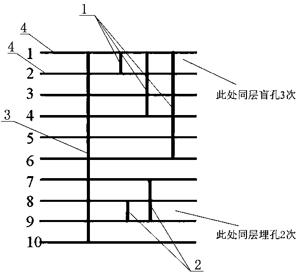
[0021] S1. The operation steps of blind buried holes in the same layer are as follows: the substrate is sequentially passed through material cutting, inner layer circuit making, inner layer etching treatment, browning treatment, pressing, blind buried hole drilling treatment, copper sinking treatment, full Board copper plating treatment, making inner layer circuit, whole board thickened copper plating treatment, film removal treatment on the outer surface of substrate, making inner layer circuit, inner layer etching treatment and browning treatment, so as to realize the one-time blind buried hole on the same layer Operation; the diameter of the blind buried hole is 0.20mm.

[0022] S2. The operation steps of blind and buried holes in the same layer twice are: stack the substrates drilled with blind and buried holes in step S1 and press them...

Embodiment 2

[0029] Embodiment two: a kind of processing technology of partial electroplating of blind buried hole, it comprises the following steps:

[0030] S1. The operation steps of blind buried holes in the same layer are as follows: the substrate is sequentially passed through material cutting, inner layer circuit making, inner layer etching treatment, browning treatment, pressing, blind buried hole drilling treatment, copper sinking treatment, full Board copper plating treatment, making inner layer circuit, whole board thickened copper plating treatment, film removal treatment on the outer surface of substrate, making inner layer circuit, inner layer etching treatment and browning treatment, so as to realize the one-time blind buried hole on the same layer Operation; the diameter of the blind buried hole is 0.29mm.

[0031] S2. The operation steps of blind and buried holes in the same layer twice are: stack the substrates drilled with blind and buried holes in step S1 and press them...


PUM

PropertyMeasurementUnit
pore sizeaaaaaaaaaa

Abstract

The invention discloses a machining process for local electroplating of blind buried holes, which comprises the following steps: S2, for two times of blind buried hole forming in the same layer, basematerials are stacked and pressed, and then blind buried hole drilling treatment, copper deposition treatment, full-board copper plating treatment, inner-layer circuit manufacturing, full-board thickened copper plating treatment, base material outer surface film stripping treatment, inner-layer circuit manufacturing, inner-layer etching treatment and browning treatment are sequentially carried out; and S3, for three times of blind buried hole forming in the same layer, the base materials are stacked and pressed, and then blind buried hole drilling treatment, copper deposition treatment, full-board copper plating treatment, inner-layer circuit manufacturing, full-board thickened copper plating treatment, base material outer surface film stripping treatment, inner-layer circuit manufacturing, inner-layer etching treatment and browning treatment are conducted in sequence. The method has the beneficial effects that when the process is applied to the forming of blind buried holes twice in the same layer, copper plating of the holes can be effectively guaranteed, and meanwhile, the problem of machining precision of small line width and small spacing is solved, and the yield is increased.

Description

technical field [0001] The invention relates to the technical field of partial blind buried hole electroplating in printed boards, in particular to a processing technology for partial blind buried hole electroplating. Background technique [0002] Printed boards are widely used in some high-power electrical equipment, power supply equipment and other fields. The circuit board needs to carry high voltage and high current to ensure normal function. At present, with the miniaturization and integration of products, the volume is getting smaller and smaller, and it is more and more difficult to process multi-layer boards with blind buried via design, especially in the same layer with multiple blind buried vias, such as ten-layer boards. Such as figure 1 As shown, the blind holes are required to be opened between layers 1-2, between layers 1-4, and between layers 1-6. Carry out copper plating treatment, and ensure that the thickness of copper plating is 20-25um. When the holes i...

Claims


Application Information

Patent Timeline
Patent Type & Authority Applications(China)
IPC IPC(8): H05K3/42C25D5/02C25D5/10
CPCH05K3/42H05K3/429H05K3/423H05K3/425C25D5/10C25D5/022
Inventor 李清华张仁军黄伟杰彭书建吴国栋
Owner 四川英创力电子科技股份有限公司
Why Eureka
Try Eureka