High-reliability image sensor wafer-level fan-out packaging structure and method

An image sensor and packaging method technology, which is applied to electric solid-state devices, semiconductor devices, radiation control devices, etc., can solve problems such as chip packaging that is not suitable for high I/O, poor reliability of the overall packaging structure, and limited signal fan-out area. , to meet the mechanical strength, solve high cost and low output, and reduce the size of the XY direction

Active Publication Date: 2020-06-30
HUATIAN TECH KUNSHAN ELECTRONICS
View PDF12 Cites 2 Cited by
  • Summary
  • Abstract
  • Description
  • Claims
  • Application Information

AI Technical Summary

Problems solved by technology

[0006] (1) The thickness of the CIS chip is limited by the height of the solder balls. In order to meet the requirements of solder ball soldering in the later stage, the thickness of the CIS chip is required to be smaller than the height of the solder balls. However, if the chip thickness is too thin, it will easily cause chip cracks and other failures;
[0007] (2) The pad signal of the CIS chip is fanned out to the surrounding edge area, but the center area cannot be equipped with RDL on the glass cover of the photosensitive area, so the signal fan-out area is limited, which is not suitable for high I / O chip packaging;
[0008] (3) There is no protective measure after the CIS chip is thinned, and the reliability of the overall packaging structure is poor. If it is used in a harsh environment, it is necessary to put forward higher requirements for the sensitivity, reliability, and durability of the chip;
[0009] (4) This packaging technology is non-wafer-level packaging, and compared with wafer-level packaging, the cost is higher

Method used


Image

  • High-reliability image sensor wafer-level fan-out packaging structure and method
  • High-reliability image sensor wafer-level fan-out packaging structure and method
  • High-reliability image sensor wafer-level fan-out packaging structure and method

Examples


specific Embodiment 1

[0120] see Figure 9-15 , A high-reliability image sensor wafer-level fan-out packaging method of the present invention includes the following steps:

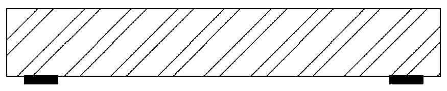
[0121] Step 1: See you Picture 9 , Thinning the CIS wafer can reduce the size after packaging, cutting the CIS wafer to obtain the CIS chip 200 to be processed, the thickness of the CIS chip is not limited, and the thinning process and the basic mechanical strength of SMT can be satisfied. Make the reliability strength of CIS chip greatly enhanced;

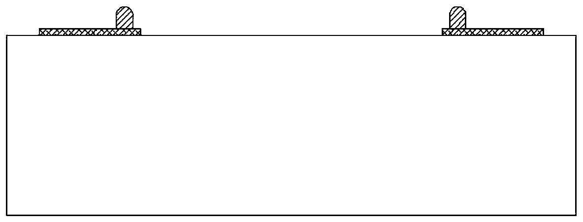
[0122] Step 2: See you Picture 10 , Provide glass substrate 100, use TGV process to perforate glass substrate 100 by wet etching or laser. TGV process can realize ultra-thin glass processing. Ultra-thin glass can reduce light refraction and reflection and increase The light transmittance, the thickness of the glass is about 150μm-200μm, and then the conductive metal is filled in the through hole 101. In this embodiment, Cu is electroplated in the through hole 101 or filled with Cu pa...

specific Embodiment 2

[0139] see Figure 7 , 8 , 9, 10, 11, 12, 13, another high-reliability image sensor wafer-level fan-out packaging method of the present invention includes the following steps:

[0140] Step 1: See you Figure 7 , Thin the CIS wafer, and cut the CIS wafer to obtain the CIS chip 200 to be processed;

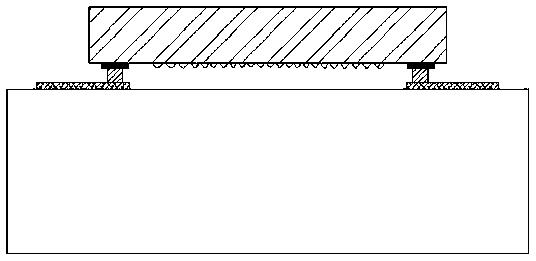
[0141] Step 2: See you Picture 10 , Provide the glass substrate 100, use the TGV process to perforate the glass substrate 100 by wet etching or laser, and then fill the conductive metal in the through hole 101. In this embodiment, Cu electroplating in the through hole 101 Or fill with Cu paste, and then form bumps 300 on the through holes 101 by photolithography and electroplating;

[0142] Step 3: See you Picture 11 , Using SMT mounting method, the CIS chip 200 and the glass substrate 100 are welded together through the pad 201 of the CIS chip and the bumps 300 on the glass substrate;

[0143] Step 4: See you Picture 12 , Using DAM dispensing technology to fill and seal the gap between...


PUM


Abstract

The invention provides a high-reliability image sensor wafer-level fan-out packaging structure and method. The high-reliability image sensor wafer-level fan-out packaging structure comprises a substrate, a CIS chip, and solder balls. A photosensitive area of the CIS chip is arranged facing one surface of the substrate and the CIS chip is connected with one surface of the substrate through an areaaround the photosensitive area, a gap at the welding position of the CIS chip and the substrate is sealed through a light shielding material, and a back surface and a side surface of the CIS chip aresubjected to integral plastic package through a plastic package layer; the solder balls are arranged on a surface of the plastic package layer, and an RDL layer of the substrate is fanned out to the surface of the plastic package layer through through holes formed in the plastic package layer and is connected with the solder balls. According to the high-reliability image sensor wafer-level fan-outpackaging structure, the problem that RDL wiring cannot be achieved due to the fact that the size of a chip is miniaturized but functions are integrated in wafer-level packaging is solved, and the problems that a traditional substrate fan-out process is high in cost and low in yield can be solved.

Description

[0001] This application claims the priority of China's earlier application, application number 2019113029655, application date 2019-12-17, and the disclosure of this patent application is incorporated herein by reference in its entirety. Technical field [0002] The invention relates to the technical field of semiconductor chips, in particular to a high-reliability image sensor wafer-level fan-out packaging structure and method. Background technique [0003] The photosensitive chip (CIS chip) is an electronic device that can sense external light and convert it into electrical signals, which is used in electronic equipment such as digital cameras and digital video cameras. The photosensitive chip is usually manufactured by a semiconductor manufacturing process, and then a series of packaging processes are performed on the photosensitive chip to form a packaged package structure. [0004] In the prior art, the fan-out package structure of the photosensitive chip mainly includes a fan-...

Claims


Application Information

Patent Timeline
Patent Type & Authority Applications(China)
IPC IPC(8): H01L21/56H01L23/31H01L27/146
CPCH01L27/14636H01L27/14683H01L23/3128H01L21/56H01L2924/181H01L2224/16225H01L2924/00012
Inventor 马书英王姣宋昆树
Owner HUATIAN TECH KUNSHAN ELECTRONICS
Why Eureka
Try Eureka