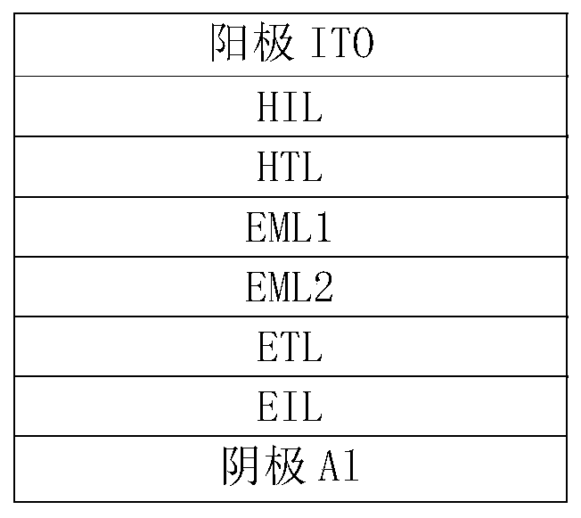
OLED device structure
An electroluminescent device, phosphorescence doping technology, applied in the direction of electric solid device, semiconductor device, semiconductor/solid state device manufacturing, etc., can solve the problems of accelerated annihilation, adverse device performance, improvement and other problems
- Summary
- Abstract
- Description
- Claims
- Application Information
AI Technical Summary
Problems solved by technology
Method used
Image

Examples
Embodiment 1
[0028] Embodiment 1 (comparative experiment)
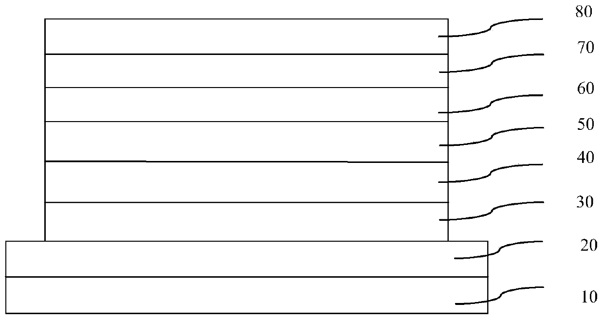
[0029] figure 1 An organic electroluminescent device that is one light-emitting layer of an OLED in the prior art
[0030] Among them, transparent conductive ITO glass substrate 10; anode 20; 3nm thick HATCN hole injection layer 30; 50nm thick TAPC hole transport layer 40; 10nm thick guest Pt-04 and host TCTA doping ratio of 20wt% as light emitting 50 nm thick TmPyPb electron transport layer 60 ; 0.8 nm LiF electron injection layer 70 ; 100 nm Al as device cathode 80 . The preparation method is the same as the preparation method of the present invention.
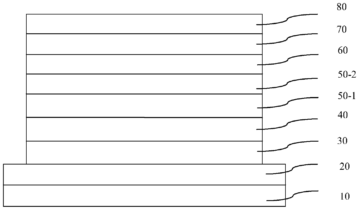
[0031] figure 2 An organic electroluminescent device that is the OLED two-layer light-emitting layer of the present application
[0032] First, the transparent conductive ITO glass substrate 10 (with the anode 20 on it) is sequentially washed with detergent solution, deionized water, ethanol, acetone, and deionized water, and then treated with oxygen plasma for 30 seconds. ...
PUM
| Property | Measurement | Unit |
|---|---|---|
| Thickness | aaaaa | aaaaa |
Abstract
Description
Claims
Application Information
 - R&D
- Intellectual Property
- Life Sciences
- Materials
- Tech Scout
- Unparalleled Data Quality
- Higher Quality Content
- 60% Fewer Hallucinations
Browse by: Latest US Patents, China's latest patents, Technical Efficacy Thesaurus, Application Domain, Technology Topic, Popular Technical Reports.
© 2025 PatSnap. All rights reserved.Legal|Privacy policy|Modern Slavery Act Transparency Statement|Sitemap|About US| Contact US: help@patsnap.com