Dielectric test system and method for micro-nano graphical film array

A dielectric testing and graphic technology, applied in the direction of dielectric performance measurement, measuring electricity, measuring devices, etc., can solve the problems of increased testing cost, expensive equipment, high testing cost, etc., and achieve high hardness, heat resistance and low temperature resistance, Avoid loss and noise, quickly test the effect of samples

Active Publication Date: 2020-07-10
SUZHOU UNIV
View PDF9 Cites 1 Cited by
  • Summary
  • Abstract
  • Description
  • Claims
  • Application Information

AI Technical Summary

Problems solved by technology

However, for large-area densely arranged patterned thin film arrays, the test efficiency of the probe method is very low; at the same time, the test process of the probe method needs to cooperate with nanoscale high-precision displacement devices, the equipment is expensive, the operation process is complicated, and the test cost is high.
In addition, adding an adjustable magnetic field and variable temperature system to the existing probe system will significantly increase the complexity of the test system and further increase the test cost
The subsequent data processing process of the probe method test also requires professional software, and the data processing process is complicated
[0006] The Chinese patent with the application number 201510047190.7 discloses a stripline resonator fixture for the dielectric performance test of the stripline method. The stripline resonator is fixed by the upper and lower clamps that cooperate with each other. The test principle belongs to the stripline method, which is suitable for larger-sized materials. During the test, the measured dielectric material needs to be filled with the space around the stripline, and it is impossible to test micro-nano-sized media with fixed geometric structures and their patterned arrays.
The Chinese patent with application number 201510047386.6 discloses a stripline method dielectric property testing system. Its test principle belongs to the stripline method and is suitable for larger-sized materials. During the test, the measured dielectric material needs to be filled around the stripline. Space, unable to test micro-nano-sized media with fixed geometry and their patterned arrays
The Chinese patent with the application number 201721136238.2 discloses a two-electrode fixture device for testing the dielectric properties of insulating material samples. The limit structure is used to adjust the electrode plate to fix the plate-shaped sample. At least 4 sets of limit screw nuts and 4 sets are required. A set of fixed screw nuts, the device has a large volume, and the flatness of the upper and lower electrode plates has not been specially optimized. It is only suitable for continuous plate-shaped samples with a large test area, and cannot accurately test micro-nano-sized media with weak electrical signals. It is beneficial to apply test conditions such as magnetic field and temperature

Method used


Image

  • Dielectric test system and method for micro-nano graphical film array
  • Dielectric test system and method for micro-nano graphical film array
  • Dielectric test system and method for micro-nano graphical film array

Examples


Embodiment 1

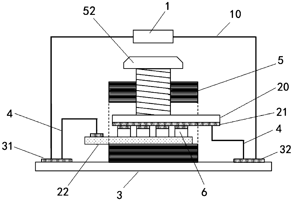
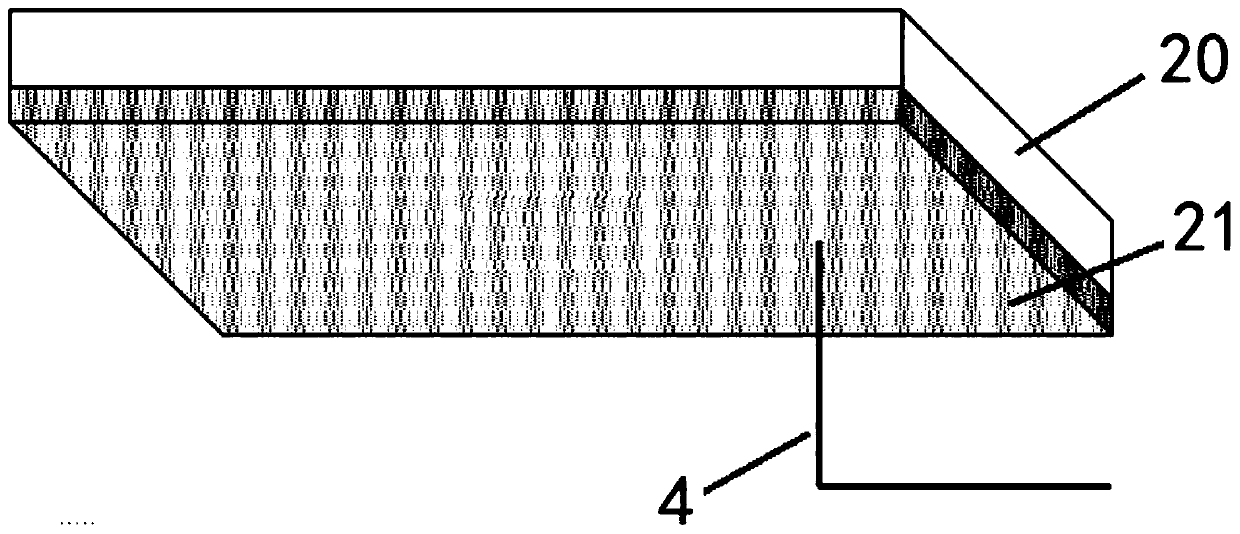
[0053] see figure 1 , a dielectric testing system for micro-nano-sized patterned film arrays according to a preferred embodiment of the present invention, comprising: a testing unit 1 for testing dielectric properties, an insulating sample stage 3, and a relatively parallel first An electrode 21, a second electrode 22 and an insulated test fixture 5 are used to sandwich a micro-nano-sized patterned film array 6 between the first electrode 21 and the second electrode 22, and the first electrode 21 and the second electrode 22 are respectively located Above and below the patterned thin film array 6 of micro-nano size.

[0054] According to the required test parameters, select the appropriate test instrument as the test unit 1.

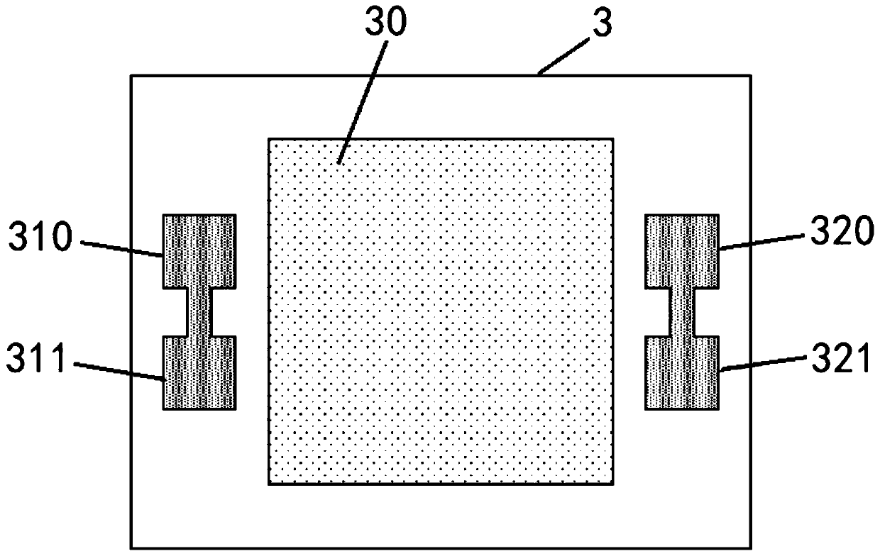
[0055] In order to reduce the influence of the weak dielectric effect of the sample stage 3 itself on the test data, the present invention uses a highly insulating material (such as Al 2 o 3 ) as the sample stage 3, using a vacuum coating method (such ...

Embodiment 2

[0064] A method for testing the dielectric properties and / or magnetodielectric properties of a micro-nano-sized patterned film array is carried out by using the dielectric testing system of Embodiment 1 of the present invention, and the steps are as follows:

[0065] Place the first electrode 21 and the second electrode 22 sandwiched with the micro-nano-sized patterned film array 6 in the sample groove 50 of the test fixture 5, and then use the fastening unit 52 to pressurize the first electrode 21 so that the first electrode 21. The micro-nano-sized patterned film array 6 and the second electrode 22 are in close contact with each other; and the test fixture 5 is placed on the sample stage 3;

[0066] Two places of the first sample stage electrode 32 on the sample stage 3 are electrically connected with the first electrode 21 and one end of the test unit 1 respectively, and two places of the second sample stage electrode 31 on the sample stage 3 are connected with the second el...


PUM

PropertyMeasurementUnit
thicknessaaaaaaaaaa
diameteraaaaaaaaaa
diameteraaaaaaaaaa

Abstract

The invention relates to a dielectric test system for a micro-nano graphical thin film array. The dielectric test system comprises a test unit, used for testing dielectric properties; an insulated sample table, provided with a first sample stage electrode and a second sample stage electrode, the first sample stage electrode and the second sample stage electrode being electrically connected with the test unit respectively; a first electrode and a second electrode which are parallel to each other, the first electrode being electrically connected with the first sample stage electrode, and the second electrode being electrically connected with the second sample stage electrode; a micro-nano graphical film array, clamped between the first electrode and the second electrode; an insulated test fixture, located on the sample table. The test fixture is provided with a sample groove used for placing the first electrode, the second electrode and the micro-nano graphical film array, the test fixture is detachably connected with an insulated fastening unit, and one end of the fastening unit is located in the sample groove and used for pressurizing the first electrode.

Description

technical field [0001] The invention relates to the field of dielectric testing devices for micro-thin films, in particular to a dielectric testing system and method for micro-nano-sized patterned thin-film arrays. Background technique [0002] Dielectric properties are an important part of material properties, and the measurement of dielectric properties can provide key information such as permittivity, dielectric loss, and magnetic permeability for many electronic applications. The dielectric properties of materials are usually tested using network analyzers, impedance analyzers, LCR meters and other instruments. According to the type of samples, they are tested in different temperature and electromagnetic field environments with specific sample test fixtures. In recent years, researchers have found that the dielectric properties of some materials will change under different applied magnetic fields, which is called the magnetodielectric properties of materials. Thin film ...

Claims


Application Information

Patent Timeline
Patent Type & Authority Applications(China)
IPC IPC(8): G01N27/22G01N27/72G01R27/26G01R31/00
CPCG01N27/221G01N27/72G01R27/2617G01R31/00
Inventor 汤如俊徐思晨
Owner SUZHOU UNIV
Why Eureka
Try Eureka