Transimpedance amplifier chip and light receiving module

A transimpedance amplifier and optical receiving technology, which is applied in the field of optical communication, can solve the problems of reducing the sensitivity performance of optical receivers, and achieve the effects of eliminating the space limitation of packaging and wiring, simplifying the packaging and wiring scheme, and improving sensitivity

Active Publication Date: 2020-07-10
MICROTERA SEMICON (GUANGZHOU) CO LTD
View PDF4 Cites 4 Cited by
  • Summary
  • Abstract
  • Description
  • Claims
  • Application Information

AI Technical Summary

Problems solved by technology

The signal in the front-end circuit of the optical receiver is connected through pins, and the exposed pins are easily interfered by external Wi-Fi signals, thereby reducing the sensitivity performance of the optical receiver

Method used


Image

  • Transimpedance amplifier chip and light receiving module
  • Transimpedance amplifier chip and light receiving module
  • Transimpedance amplifier chip and light receiving module

Examples


Embodiment 1

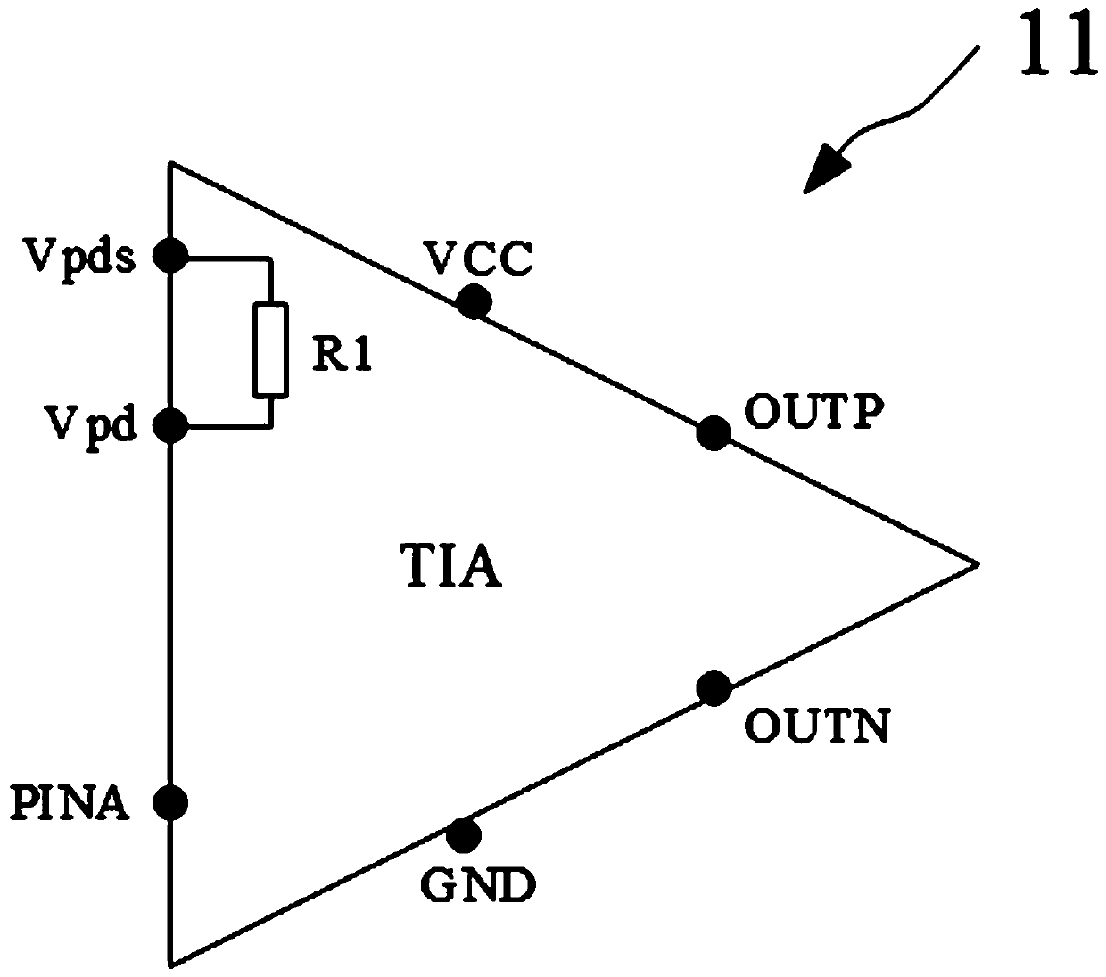
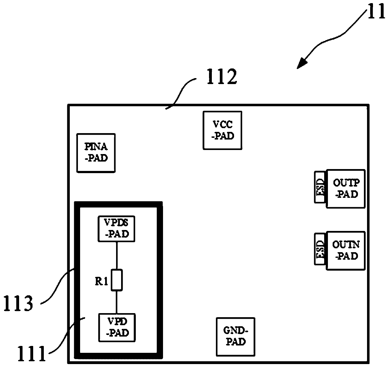
[0038] Such as Figure 2~Figure 4 As shown, the present embodiment provides a transimpedance amplifier chip 11 , in which the filter resistor R1 is integrated into the transimpedance amplifier chip 11 and corresponding pads are provided. The transimpedance amplifier chip 11 includes:

[0039] A filter resistor region 111 , a transimpedance amplifier device region 112 and a deep trench 113 are built in.

[0040] Such as image 3 and Figure 4 As shown, a filter resistor R1 is formed in the built-in filter resistor region 111 .

[0041]Specifically, the filter resistor R1 is formed on the substrate and is not electrically connected to the substrate (that is, an insulating material layer is provided between the filter resistor R1 and the substrate). As an example, the material of the filter resistor R1 includes Poly or Tin, wherein the withstand voltage of Poly can reach 200V, and any material with a withstand voltage greater than the voltage value of the bias voltage Vapd is...

Embodiment 2

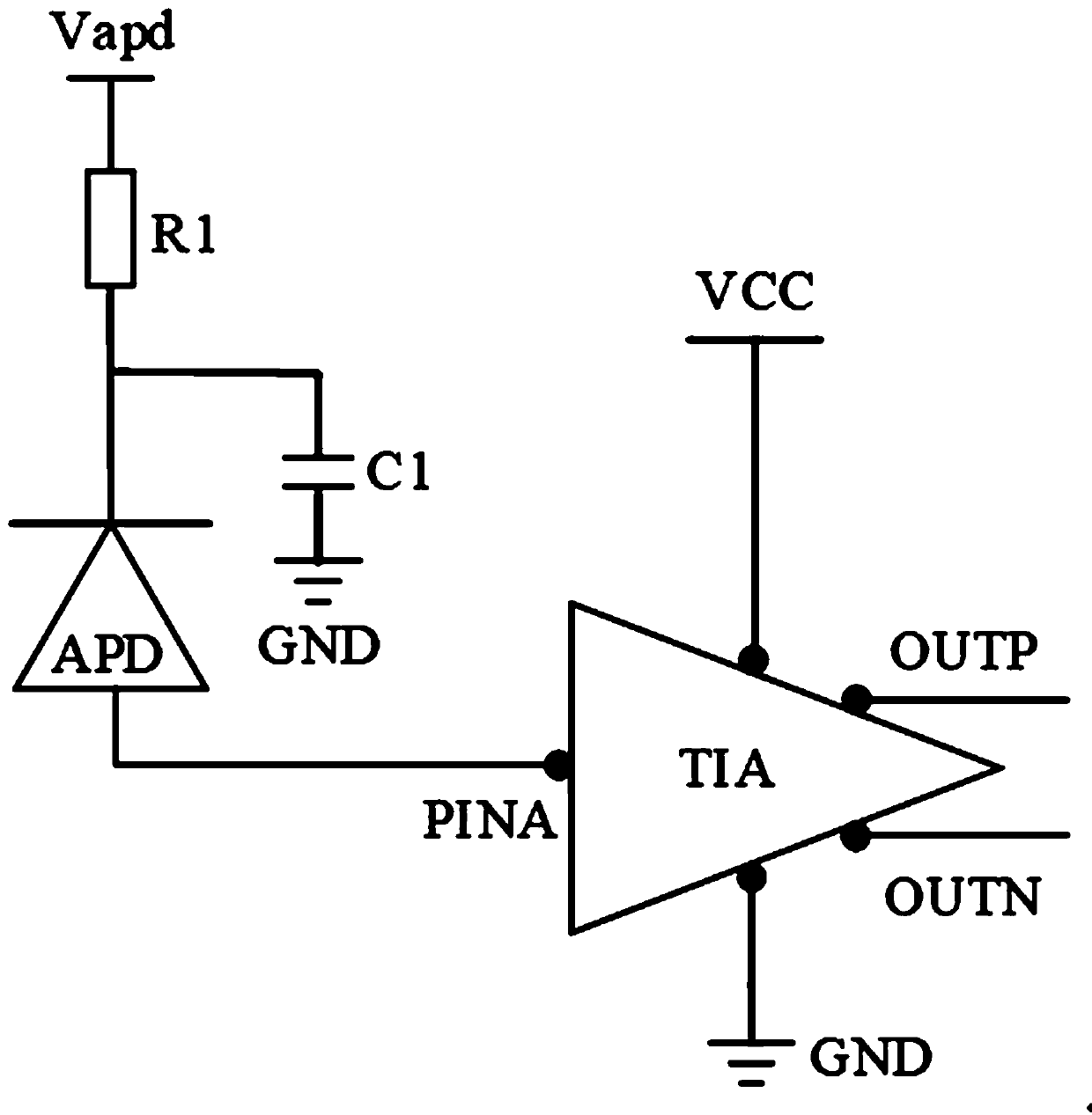
[0054] Such as Figure 5 As shown, this embodiment provides a light receiving module 1, the light receiving module 1 includes:

[0055] The photodetector, filter capacitor C1 and transimpedance amplifier chip 11 packaged in the same package.

[0056] Such as Figure 5 As shown, the two ends of the photodetector are respectively connected to the photocurrent input terminal PINA of the transimpedance amplifier chip 1 and the first terminal Vpd of the filter resistor R1 in the transimpedance amplifier chip 1 through corresponding pads.

[0057] Specifically, as an example, the photodetector adopts a photodiode PD, the cathode of the photodiode PD is connected to the first terminal Vpd of the filter resistor R1, and the anode of the photodiode PD is connected to the light source of the transimpedance amplifier. Current input PINA. The photodiode PD is preferably an avalanche photodiode APD, and a larger current signal can be obtained through the photoelectric effect of the aval...


PUM


Abstract

The invention provides a transimpedance amplifier chip and a light receiving module. The transimpedance amplifier chip comprises a photoelectric detector, a filter capacitor and a transimpedance amplifier chip which are packaged in the same packaging body, wherein the trans-impedance amplifier chip comprises a built-in filter resistor region and a trans-impedance amplifier device region which areisolated through a deep trench, a filter resistor is formed in the built-in filter resistor region, two ends of the filter resistor are led out to corresponding bonding pads through metal layer leads,and the built-in filter resistor and each metal layer in the built-in filter resistor region are not connected with a substrate; and devices forming a transimpedance amplifier are formed in the transimpedance amplifier device region. According to the invention, the filter circuit formed by the filter capacitor and the filter resistor is added to reduce the influence of an external Wi-Fi signal onan optical receiver and improve the sensitivity of the optical receiver; the filter resistor is arranged in the trans-impedance amplifier chip, so that the use cost of the off-chip resistor is saved,the space limitation of packaging and routing is eliminated, the packaging and routing scheme is simplified, and the practical value is high.

Description

technical field [0001] The invention relates to the technical field of optical communication, in particular to a transimpedance amplifier chip and an optical receiving module. Background technique [0002] Optical communication technology is a communication method that uses light waves as the transmission medium. Both light waves and radio waves are electromagnetic waves, but the frequency of light waves is higher than that of radio waves, and the wavelength is shorter than that of radio waves. Therefore, it has the advantages of wide transmission frequency, large communication capacity and strong anti-electromagnetic interference ability. [0003] Optical communication mainly includes optical transmitter, optical fiber and optical receiver. Among them, the role of the optical transmitter is to convert the HDB3 signal code sent from the multiplexing equipment into NRZ code; then encode the NRZ code into a code pattern suitable for transmission on the optical cable line; T...

Claims


Application Information

Patent Timeline
Patent Type & Authority Applications(China)
IPC IPC(8): H03F3/10H03F1/52
CPCH03F1/52H03F3/10
Inventor 刘森刘盛富刘筱伟杨超刘海彬胡云斌
Owner MICROTERA SEMICON (GUANGZHOU) CO LTD
Why Eureka
Try Eureka