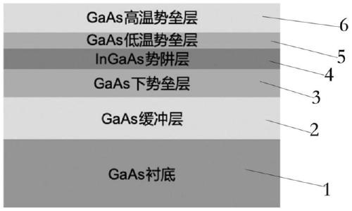
Quantum well structure and growth method thereof
A growth method and quantum well technology, which is applied in the field of semiconductor materials, can solve problems affecting film deposition, reduce In incorporation rate, and a large number of In vacancies, so as to improve growth quality, optimize growth temperature, and improve crystal quality and optical properties. Effect
- Summary
- Abstract
- Description
- Claims
- Application Information
AI Technical Summary
Problems solved by technology
Method used
Image

Examples
Embodiment 1
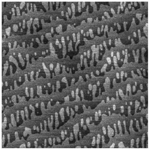
[0072] In this embodiment, the InGaAs / GaAs quantum well structure is grown by MOCVD equipment, wherein the GaAs lower barrier layer growth temperature T 1 is 650℃, and the potential well layer is In 0.25 GaAs, the thickness is 8nm, the growth temperature is T 2 It is 540°C. The growth temperature of the GaAs upper barrier layer is the same as 540°C, and the thickness is 20nm, that is, in this embodiment, the GaAs upper barrier layer is not grown at a variable temperature, but isothermally grown, T 2 =T 3 = 540°C. figure 2 It is the atomic force microscope test result of the surface of the barrier layer on the isothermally grown GaAs, the surface roughness is 0.143nm, the surface step spacing is small, about 32nm, and there are many small two-dimensional islands distributed on these mesas, indicating that the two-dimensional Layered growth mode and step flow growth mode coexist. However, the step-flow growth mode is the best growth mode to obtain a complete lattice struct...
Embodiment 2
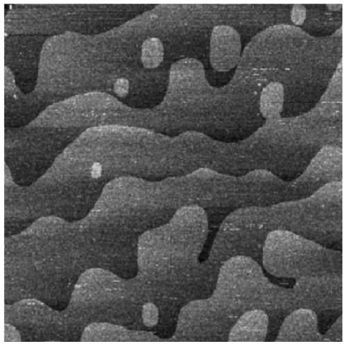
[0074] In this embodiment, the InGaAs / GaAs quantum well structure is grown by MOCVD equipment, wherein the GaAs lower barrier layer growth temperature T 1 is 650℃, and the potential well layer is In 0.25 GaAs, growth temperature T 2 is 540°C, the growth temperature of the GaAs low-temperature barrier layer is also 540°C, and the thickness h 1 2nm, GaAs high temperature barrier layer growth temperature T 3 650°C, thickness h 2 18nm. image 3 The atomic force microscope test results of the surface of the barrier layer on GaAs grown at variable temperature, the surface roughness is 0.128nm, the surface step spacing is wide, about 49nm, and there are only a few two-dimensional islands on the step surface, and the size is relatively large, indicating that the large Most atoms choose the step flow growth mode, and very few choose the two-dimensional layered growth mode. It can be seen that temperature affects the choice of atoms for nucleation sites. From a thermodynamic point...
Embodiment 3
[0076] In this embodiment, the InGaAs / GaAs quantum well structure is grown by MOCVD equipment, wherein the GaAs lower barrier layer growth temperature T 1 is 650℃, and the potential well layer is In 0.25 GaAs, growth temperature T 2 is 560°C, the growth temperature of the GaAs low-temperature barrier layer is also 560°C, and the thickness h 1 2nm, GaAs high temperature barrier layer growth temperature T 3 650°C, thickness h 2 18nm. Image 6 The atomic force microscope test results of the surface of the barrier layer on the variable temperature grown GaAs show that the surface steps are equidistant, with an interval of about 30nm, and there are no two-dimensional islands, indicating that it has completely transformed into a step flow growth mode at this time. Figure 5It is the X-ray diffraction test result of the InGaAs / GaAs quantum well structure, and interference fringes appear in the diffraction peak of InGaAs, indicating that the crystalline quality of the InGaAs poten...
PUM
| Property | Measurement | Unit |
|---|---|---|
| Growth temperature | aaaaa | aaaaa |
| Growth temperature | aaaaa | aaaaa |
| Thickness | aaaaa | aaaaa |
Abstract
Description
Claims
Application Information
 - Generate Ideas
- Intellectual Property
- Life Sciences
- Materials
- Tech Scout
- Unparalleled Data Quality
- Higher Quality Content
- 60% Fewer Hallucinations
Browse by: Latest US Patents, China's latest patents, Technical Efficacy Thesaurus, Application Domain, Technology Topic, Popular Technical Reports.
© 2025 PatSnap. All rights reserved.Legal|Privacy policy|Modern Slavery Act Transparency Statement|Sitemap|About US| Contact US: help@patsnap.com