
Pixel-level high-speed narrow-pulse peak holding circuit
A peak hold circuit and narrow pulse technology, which is applied in pulse processing, pulse technology, electrical components, etc., can solve the problems of large power consumption and large area, and achieve the effects of low power consumption, high holding accuracy, and small occupied area
- Summary
- Abstract
- Description
- Claims
- Application Information
AI Technical Summary
Problems solved by technology
Method used
Image

Examples
Embodiment 1
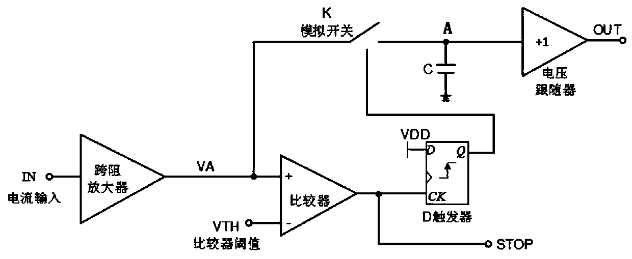
[0021] Such as figure 1 As shown, the pixel-level high-speed narrow pulse peak hold circuit includes a transimpedance amplifier, a comparator, a D flip-flop, an analog switch K, a holding capacitor C and a voltage follower. Transimpedance Amplifiers and Comparators The transimpedance amplifiers and comparators of the lidar readout circuit can be utilized. The input terminal of the transimpedance amplifier is connected to the current signal IN, the output terminal is connected to the non-inverting input terminal of the comparator, the inverting input terminal is connected to the threshold voltage VTH of the comparator, the output terminal of the comparator generates a digital signal STOP, and the digital signal STOP is connected to the D trigger at the same time The clock signal end of the D flip-flop, the D end of the D flip-flop is connected to the power supply VDD, the output end of the D flip-flop is connected to the analog switch K, the output end of the transimpedance amp...
Embodiment 2
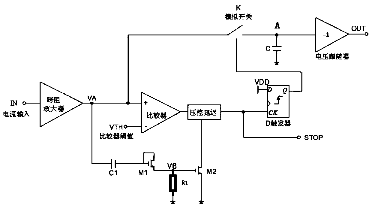
[0025] Such as figure 2 As shown, on the basis of Embodiment 1, a voltage-controlled delay unit, a capacitor C1, MOS transistors M1, M2 and a resistor R1 are added.
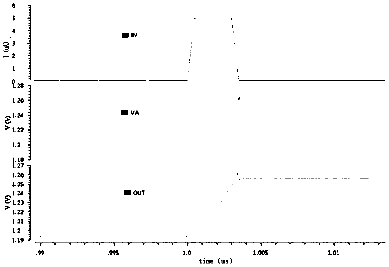
[0026] Usually, the transimpedance amplifier needs to work in the linear region to ensure that the output voltage VA and the input current IN have a linear relationship. At this time, the pulse width of the input current IN is basically the same as the pulse width of the output voltage VA. However, when the input current IN is large, the transimpedance amplifier works in the nonlinear region, the voltage amplitude of VA is large, and the rising edge and pulse width of VA change.
[0027] At the output terminal VA of the transimpedance amplifier, add a capacitor C1, a plurality of series-connected gate-drain short-circuited MOS transistors M1, resistor R1, and MOS transistor M2 to sense the large-value voltage output at the VA terminal; at the output terminal of the comparator A voltage-controlled delay unit is...
PUM
 Abstract
Description
Claims
Application Information