Temperature control method and system, semiconductor device

A temperature control method and technology of a temperature control system, which are applied in the fields of semiconductor devices, semiconductor/solid-state device manufacturing, and vacuum evaporation plating, etc., can solve problems such as the reduction of heating efficiency, reduce broken disks, reduce fluctuations in heating power, Guaranteed heating rate effect

A temperature control method and technology of a temperature control system, which are applied in the fields of semiconductor devices, semiconductor/solid-state device manufacturing, and vacuum evaporation plating, etc., can solve problems such as the reduction of heating efficiency, reduce broken disks, reduce fluctuations in heating power, Guaranteed heating rate effect

CN111501004BActive Publication Date: 2022-06-17BEIJING NAURA MICROELECTRONICS EQUIP CO LTD

Image

  • Temperature control method and system, semiconductor device
  • Temperature control method and system, semiconductor device
  • Temperature control method and system, semiconductor device

Examples


Embodiment Construction

[0037] In order for those skilled in the art to better understand the technical solutions of the present invention, the temperature control method, system and semiconductor device provided by the present invention are described in detail below with reference to the accompanying drawings.

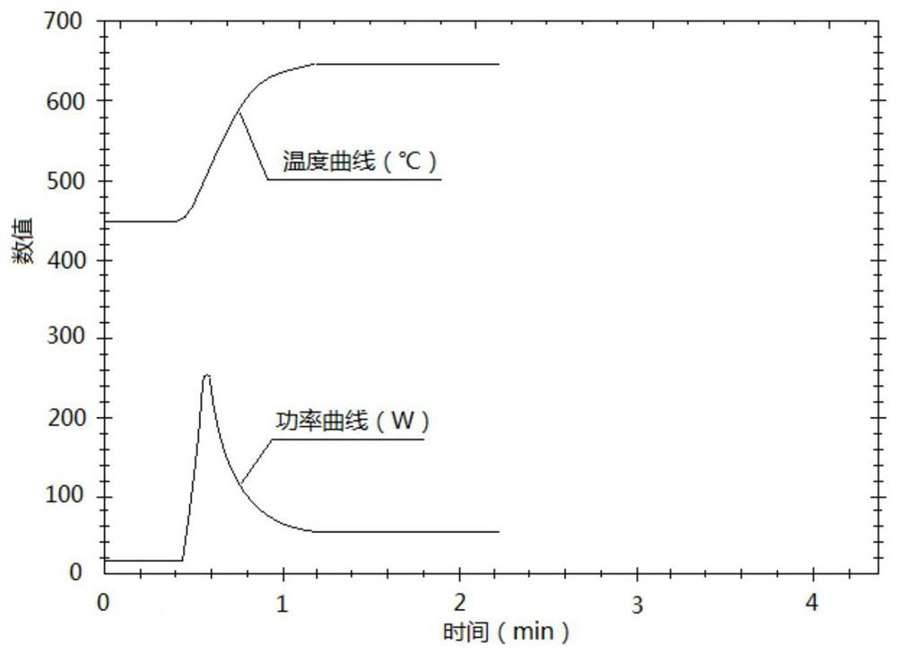
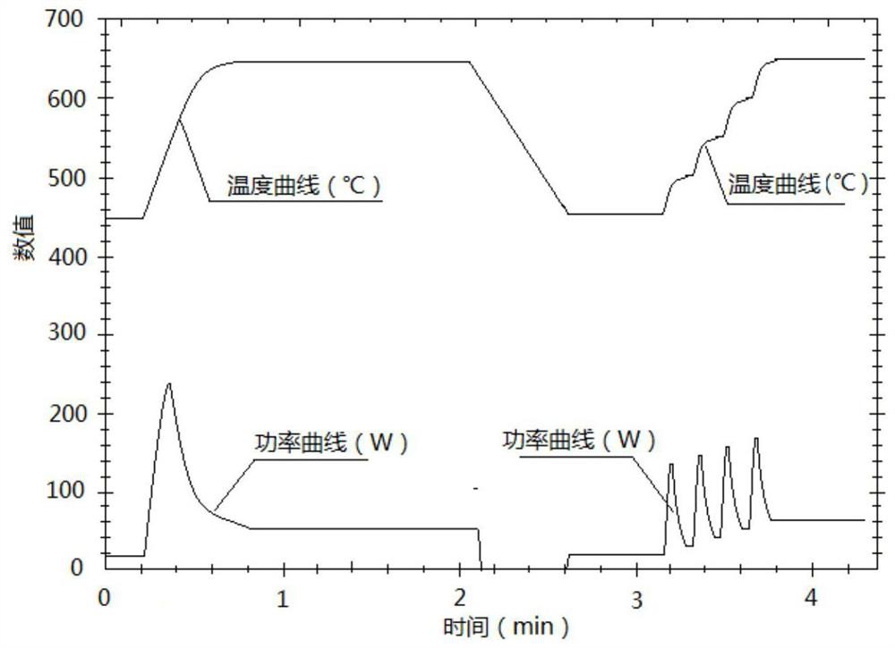
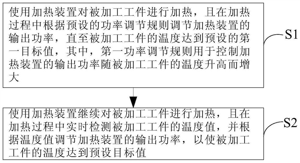
[0038] see image 3 , an embodiment of the present invention provides a temperature control method for a semiconductor device, which includes:

[0039] Step S1, use a heating device to heat the workpiece to be processed, and adjust the output power of the heating device according to a preset power regulation rule during the heating process, until the temperature of the workpiece to be processed reaches a preset first target value, wherein, The above-mentioned first power regulation rule is used to control the output power of the heating device to increase as the temperature of the workpiece to be processed increases;

[0040] Step S2, use the heating device to continue to heat the workpiece...


PUM


Abstract

The present invention provides a temperature control method and system, and semiconductor equipment. The method includes the following steps: S1, use a heating device to heat the workpiece to be processed, and adjust the output power of the heating device according to a preset power adjustment rule during the heating process , until the temperature of the processed workpiece reaches the preset first target value, wherein the first power adjustment rule is used to control the output power of the heating device to increase as the temperature of the processed workpiece increases; S2, using the heating device to continue to The processed workpiece is heated, and the temperature value of the processed workpiece is detected in real time during the heating process, and the output power of the heating device is adjusted according to the temperature value, so that the temperature of the processed workpiece reaches a preset target value. The technical solution of the temperature control method and system provided by the present invention can reduce the fluctuation of heating power and effectively reduce the occurrence of broken disks on the basis of ensuring the heating rate.

Description

technical field [0001] The present invention relates to the technical field of semiconductor processing, and in particular, to a temperature control method and system, and semiconductor equipment. Background technique [0002] In the manufacturing process of LEDs such as blue light, white light, etc., gallium nitride (GaN) is directly epitaxially grown on a sapphire substrate, and there has always been a problem of lattice mismatch and thermal mismatch. Since the aluminum nitride (AlN) material has the same lattice structure as GaN, and also has a strong degree of matching with the lattice of the sapphire material, AlN is used as a buffer layer and placed between the sapphire substrate and GaN. There is a great improvement in reducing epitaxial defects and improving epitaxial quality. [0003] At present, an aluminum nitride sputtering equipment is usually used to deposit an aluminum nitride film on a sapphire substrate by physical vapor deposition (Physical VaporDeposition...

Claims


Application Information

Patent Timeline
17 Jun 2022
Publication
CN111501004B
IPC
H01L21/00
CPC
C23C14/54; C23C14/35; C23C14/0617; H01L33/007; H01L33/12
Inventors
刘玉杰; 文莉辉