Three-dimensional conductive circuit and preparation method thereof
A conductive circuit and three-dimensional technology, which is applied in the direction of printed circuit manufacturing, printed circuit, conductive pattern formation, etc., can solve the problems of complicated process and long production cycle, and achieve the effect of simple process, low cost and high efficiency
- Summary
- Abstract
- Description
- Claims
- Application Information
AI Technical Summary
Problems solved by technology
Method used
Image

Examples
Embodiment 1
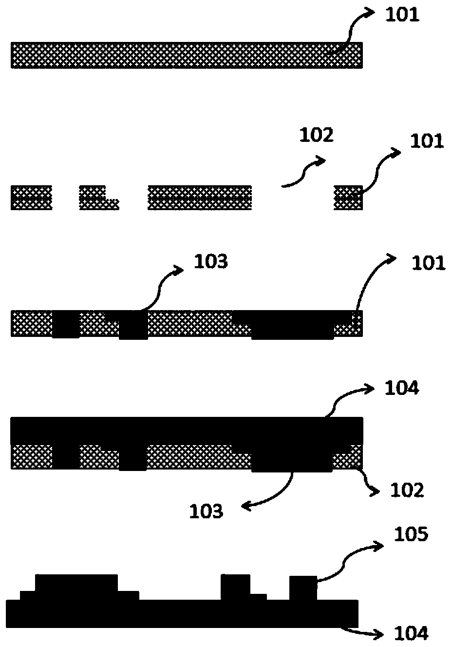
[0039] A preparation method of a three-dimensional conductive circuit: as figure 1 Shown:
[0040] S1: making a groove 102 in the organic material layer 101 that conforms to the designed circuit pattern, and the depth of the groove is 1-1.25 times the height of the conductive circuit;
[0041] Groove 102 can be made groove 102 by the method of direct printing or spraying, and organic material layer 101 is the organic material layer that contains ester group and can alkali retreat, and the thermal decomposition temperature of organic material layer is lower than the heat treatment temperature of described conductive paste ;
[0042] S2: Fill the three-dimensional groove 102 with conductive paste 103, the conductive paste 103 is conductive aluminum paste, and paste the high-temperature-resistant substrate 104 on the graphics surface filled with the conductive paste 103, and the high-temperature-resistant substrate 104 is alumina ceramics , and further heat and strengthen the c...
Embodiment 2
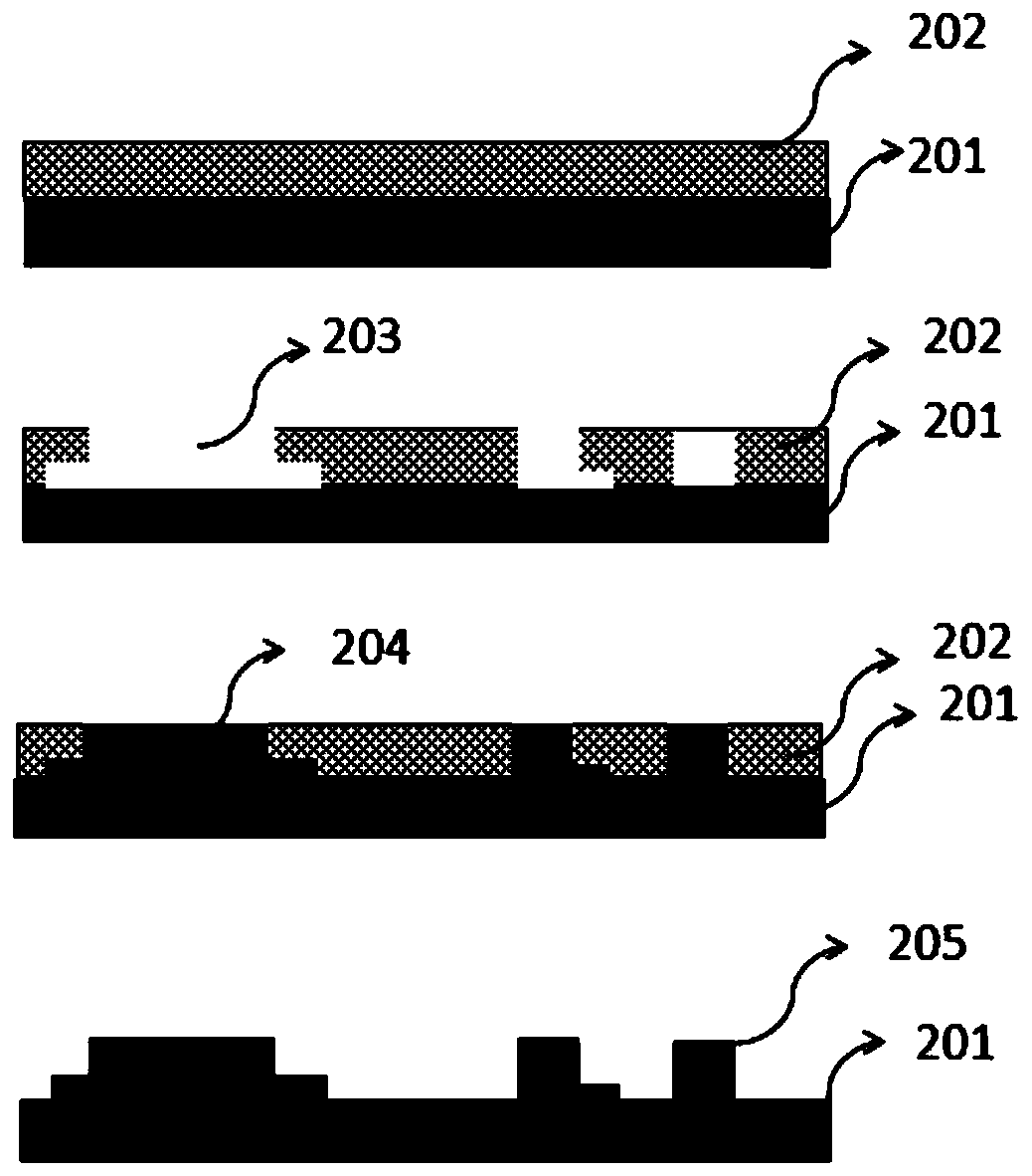
[0046] A preparation method of a three-dimensional conductive circuit: as figure 2 Shown:
[0047] S1: Coating an organic material layer on the surface of the high-temperature-resistant substrate 201 and curing the organic material layer 202, making a groove 203 in the organic material layer 202 that conforms to the designed circuit pattern, and the depth of the groove is 1-1.25 times the height of the conductive circuit;
[0048] The groove 203 can be made by exposure and development. The organic material layer 202 is a photoresist film. The thermal decomposition temperature of the organic material layer is lower than the heat treatment temperature of the conductive paste. The high temperature resistant substrate 201 is single crystal silicon ;
[0049] S2: filling the three-dimensional groove 203 with conductive paste 204, the conductive paste 204 is conductive silver paste, curing the conductive paste to make it lose fluidity; photocuring the conductive paste;
[0050] S...
Embodiment 3
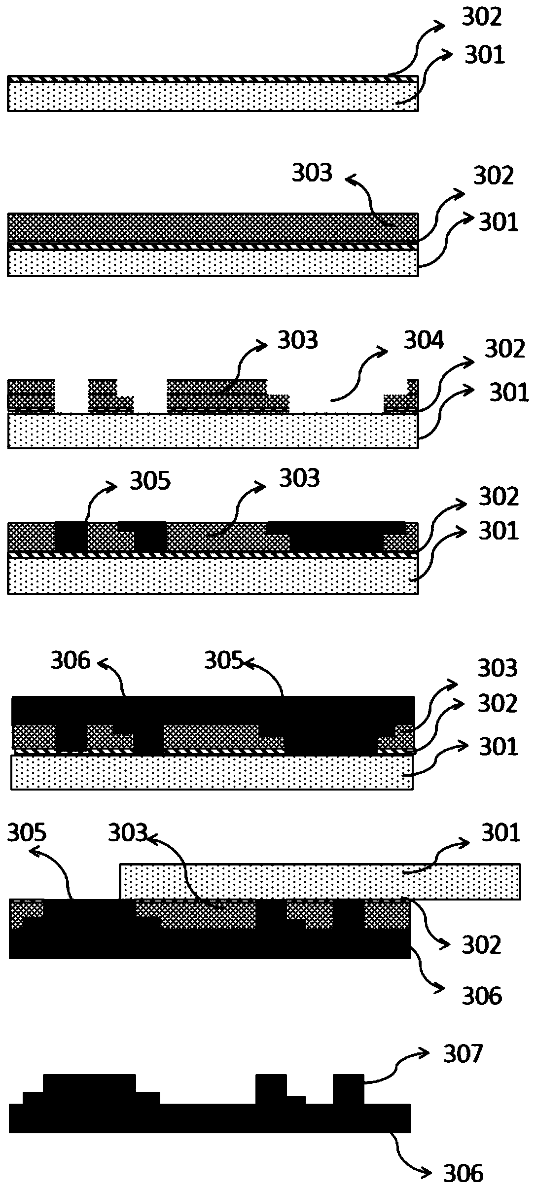
[0053] A preparation method of a three-dimensional conductive circuit: as image 3 Shown:
[0054] S1: Coating a thermal slip adhesive layer 302 on the surface of a common substrate 301, coating an organic material layer with a certain thickness on the surface of the thermal slip adhesive layer 302 and curing the organic material layer 303; the organic material layer 303 is a photoresist film, the thermal decomposition temperature of the organic material layer is lower than the heat treatment temperature of the conductive paste; the common base material 301 can be selected from epoxy resin;
[0055] S2: Make a groove 304 in the organic material layer 301 that conforms to the designed circuit pattern. The groove 304 can be made by laser or mechanical engraving. The depth of the groove is 1-1.25 times the height of the conductive circuit;
[0056] S3: Fill the three-dimensional groove with conductive paste 305, the conductive paste 305 is conductive copper paste, and paste the ...
PUM
 Abstract
Description
Claims
Application Information
 - R&D
- Intellectual Property
- Life Sciences
- Materials
- Tech Scout
- Unparalleled Data Quality
- Higher Quality Content
- 60% Fewer Hallucinations
Browse by: Latest US Patents, China's latest patents, Technical Efficacy Thesaurus, Application Domain, Technology Topic, Popular Technical Reports.
© 2025 PatSnap. All rights reserved.Legal|Privacy policy|Modern Slavery Act Transparency Statement|Sitemap|About US| Contact US: help@patsnap.com