Micro pressure sensor chip and preparation method thereof

A micro-pressure sensor and chip technology, applied in piezoelectric/electrostrictive/magnetostrictive devices, instruments, microstructure technology, etc., can solve the problem of susceptibility to the influence of parasitic capacitance, increase of sensor nonlinearity, and increase of signal processing Difficulty and other issues, to achieve the effect of easy processing, good linearity and low cost

Active Publication Date: 2022-05-31
陕西省计量科学研究院 +1
View PDF1 Cites 0 Cited by
  • Summary
  • Abstract
  • Description
  • Claims
  • Application Information

AI Technical Summary

Problems solved by technology

[0003] Pressure sensors with different sensitivity principles have their own advantages and disadvantages: for example, piezoelectric sensors are limited by their sensitivity principles and cannot measure static pressure, and the output charge signal needs to be processed by subsequent complex auxiliary circuits; capacitive pressure sensors have high sensitivity, The temperature drift is small, the power consumption is low, but the input impedance is large, it is easily affected by the parasitic capacitance, and it is more sensitive to the interference of the surrounding environment; the resonant pressure sensor has better sensitivity and lower temperature drift, but the process is complex, Low yield rate is its shortcoming; although the piezoresistive pressure sensor is greatly affected by temperature, it has a wide measurement range, can measure static and dynamic signals, has high precision, good dynamic response, and simple post-processing circuit
As the thickness of the stress film structure decreases, the sensitivity of the sensor to pressure will increase, but the nonlinearity of the sensor will also increase, thus increasing the difficulty of signal processing

Method used


Image

  • Micro pressure sensor chip and preparation method thereof
  • Micro pressure sensor chip and preparation method thereof
  • Micro pressure sensor chip and preparation method thereof

Examples


Embodiment Construction

[0045] In order to make the purpose and technical solutions of the present invention clearer and easier to understand. Below in conjunction with the accompanying drawings and examples,

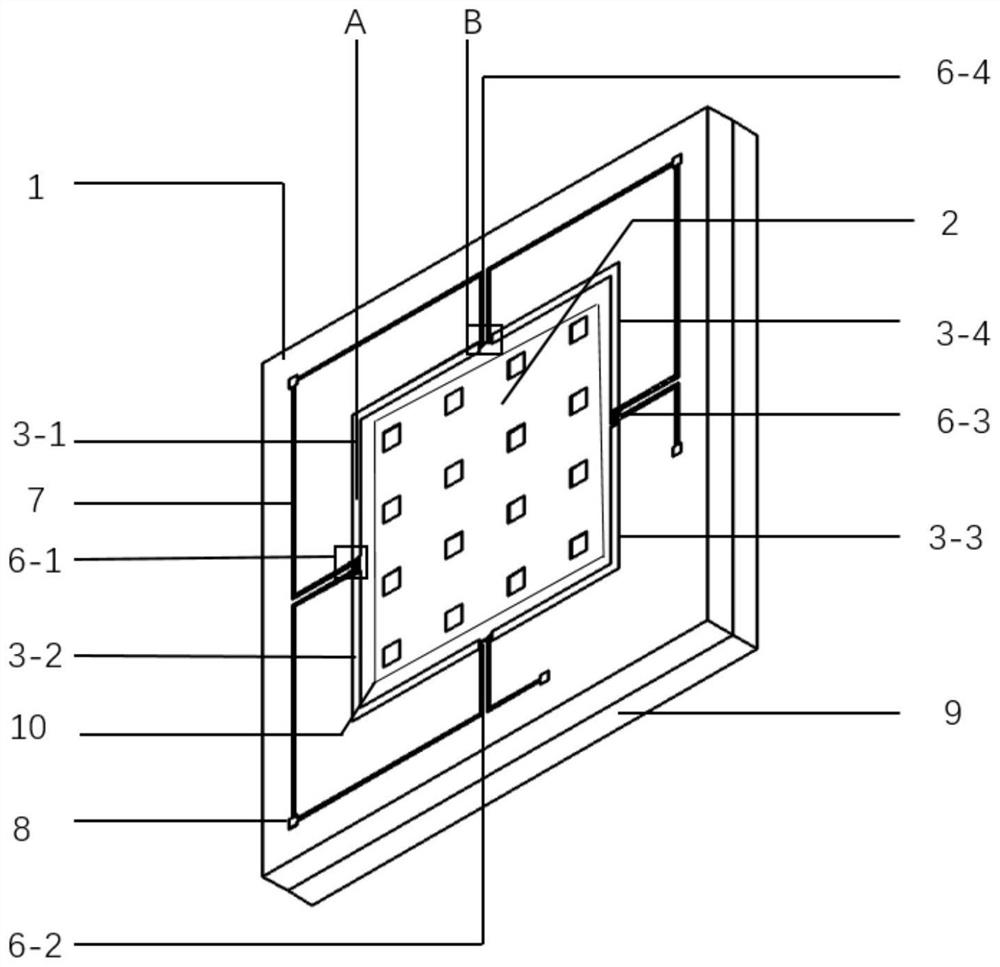
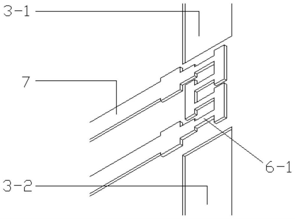
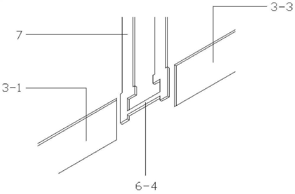
[0050] The depth of the stress adjustment grooves in the array 10 is 20% to 80% of the thickness of the stress film 2 . The first stress concentration groove to the first

[0062] 7) Referring to FIG. 7g, the back surface of the substrate 1 is bonded to the top surface 11 of the anti-overload glass 9 to obtain a micro-pressure sensor chip.

[0064] FIG. 8 is a schematic diagram of the cross-sectional structure relationship of the present invention in an unloaded state. Referring to Figure 9, the sensor is at a slight pressure P

[0074] 7. Chip shape: 5mm×5mm.


PUM

PropertyMeasurementUnit
Sensitivityaaaaaaaaaa

Abstract

The invention discloses a micro-pressure sensor chip and a preparation method thereof. The main components of the sensor chip include a stress film, a base, a piezoresistive strip, metal leads, an overload protection component and the like. The specific structure is to make a stress film with stress adjustment grooves and stress concentration grooves on the chip structure substrate. Four stress concentration grooves are evenly distributed on the edge of the stress film, four piezoresistor strips are arranged between the ends of two adjacent stress concentration grooves, and metal leads connect the piezoresistor strips to form a semi-open-loop Wheatstone bridge. The gap between the cross support beam and the bump in the back cavity of the chip further improves the stress concentration effect at the varistor strip; the main preparation process includes: making the varistor strip on the cleaned SOI silicon wafer, and then using P Type heavy doping to make ohmic contact area, then make metal leads and pads, dry etch stress concentration grooves and stress adjustment grooves, then make the back cavity structure of the chip, and finally bond the fabricated chip structure substrate with the anti-overload glass Bond.

Description

Micro pressure sensor chip and preparation method thereof technical field The invention belongs to MEMS piezoresistive micro-pressure sensor technical field, be specifically related to a kind of micro-pressure sensor chip and its Preparation. Background technique [0002] The current MEMS micro-pressure sensor has been widely used in biomedical, aerospace, wind tunnel testing and other fields, especially It is used in the aerospace field, which has strict requirements on the size, weight, sensitivity and natural frequency of the sensor. MEMS transmission Sensors are widely used because of their small size and high precision. For example, in the field of medical devices, cardiovascular automatic testers are used. The micro pressure sensor is used as a measurement sensitive element to measure the radial artery information. In order to ensure the accuracy of the diagnosis, the micro pressure sensor is accurate. High requirements are placed on the stability and repeatab...

Claims


Application Information

Patent Timeline
Patent Type & Authority Patents(China)
IPC IPC(8): G01L1/20G01L9/02B81B7/02B81C1/00
CPCG01L1/20G01L9/02B81B7/02B81C1/00015B81B2201/0264
Inventor 王鸿雁赵立波吴永顺魏于昆山涛皇咪咪徐廷中陈翠兰李学琛蒋庄德
Owner 陕西省计量科学研究院
Why Eureka
Try Eureka