Gain device based on micro-nano structure semiconductor film and laser

A micro-nano structure and semiconductor technology, applied in the field of lasers, can solve the problems affecting the output power and efficiency of lasers, the inability to achieve high beam quality output, and the inability to solve laser total reflection well, so as to improve laser efficiency, realize beam quality, The effect of the large model field

Active Publication Date: 2020-08-11
NAT UNIV OF DEFENSE TECH
View PDF8 Cites 0 Cited by
  • Summary
  • Abstract
  • Description
  • Claims
  • Application Information

AI Technical Summary

Problems solved by technology

[0004] At present, most high-power semiconductor lasers are electrically excited edge-emitting lasers. The electro-optic conversion efficiency of this type of laser can reach about 70%. However, due to the large divergence angle of edge-emitting lasers, it is impossible to achieve high beam quality output. The light emitting vertical external cavity surface emitting laser (VECSEL) can achieve high beam quality and large mode field lasing
However, such lasers are currently unable to achieve high power output, and the main limiting factor is still the influence of thermal effects. Under high power operating conditions, the waste heat generated by the semiconductor gain layer cannot be quickly dissipated through the heat sink, which affects the output power and efficiency of the laser.
Removing the distributed Bragg reflection (DBR) layer in such lasers is an effective way to improve heat dissipation efficiency, but after removing the DBR layer, the total reflection of the laser perpendicular to the surface of the gain medium cannot be solved well

Method used


Image

  • Gain device based on micro-nano structure semiconductor film and laser
  • Gain device based on micro-nano structure semiconductor film and laser
  • Gain device based on micro-nano structure semiconductor film and laser

Examples


Embodiment 1

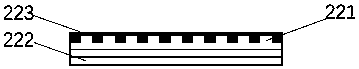
[0067] This embodiment provides a semiconductor thin film with micro-nano structure, such as figure 1 As shown, from top to bottom, including window layer 223, microstructure layer 221 and multiple quantum well layer 222;

[0068] The multi-quantum well layer 222 includes four stacked barrier layers GaAs (each barrier layer GaAs (gallium arsenide) has a thickness of 250 nm) and three well layers InGaAs (each well layer InGaAs (indium gallium arsenide) ) with a thickness of 10 nm), the well layer is located between different barrier layers;

[0069] The microstructure layer 221 is a one-dimensional grating structure with a grating period of 550 nm, a duty ratio of 0.5, and an etching depth of 300 nm.

[0070] The material of the window layer 223 is SiO 2 , with a thickness of 5 nm. The window layer 223 is located on the upper end of the micro-nano-structured semiconductor film 22 and plays a role of protecting the micro-structured layer 221 .

[0071] In this embodiment, th...

Embodiment 2

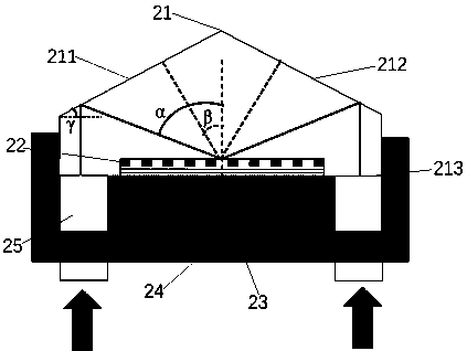
[0073] This embodiment provides a gain device based on a micro-nano-structured semiconductor thin film, such as figure 2 As shown, it includes a prism window 21 and a micro-nano-structured semiconductor film 22 as described in Embodiment 1;

[0074] The prism window 21 includes a bottom surface 213 and a pair of inclined surfaces (the first inclined surface 211 and the second inclined surface 212) inclined relative to the bottom surface; a pair of the inclined surfaces are symmetrically distributed on the bottom surface 213, and the inclined surfaces The angles are +45º and -45º respectively; the inclined surfaces are coated with a set of film systems to achieve the purpose of reflecting the pumping light and transmitting the oscillating light;

[0075] The upper end of the micro-nano-structured semiconductor film 22 is bonded to the bottom surface 213 of the prism window 21 through photoresist technology to improve the heat dissipation efficiency of the micro-nano-structured...

Embodiment 3

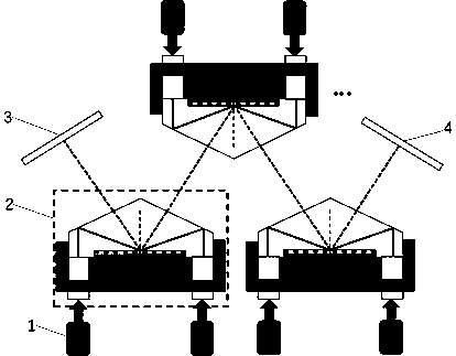
[0080] This embodiment provides a laser based on a micro-nano-structured semiconductor thin film, such as image 3 shown, including:

[0081] The active mirror group includes three active mirrors 2, and the active mirror 2 includes a gain device, a base 23, a heat sink 24 and a focusing lens 25 as described in Embodiment 2; one end of the base 23 is connected to the The lower end of the micro-nano structure semiconductor film 22 is pasted and fixed by optical glue technology, and the other end of the substrate 23 is fixedly connected to the heat sink 24 by an indium film welding process; each active mirror 2 includes two focusing lenses 25 , the focusing lens 25 is symmetrically distributed on the side of the substrate 23, the focusing lens 25 passes through the heat sink 24 and is fixedly installed on the heat sink 24; one end of the focusing lens 25 is close to the pump source 1. The other end is close to the bottom surface 213 of the prism window 21, and the pumping light ...


PUM

PropertyMeasurementUnit
thicknessaaaaaaaaaa
thermal conductivityaaaaaaaaaa
thicknessaaaaaaaaaa

Abstract

The invention discloses a gain device based on a micro-nano structure semiconductor film and a laser. The micro-nano structure semiconductor film comprises a window layer (223), a micro-structure layer (221) and a multi-quantum well layer (222) from top to bottom. The multi-quantum well layer (222) comprises at least two barrier layers, and a well layer is arranged between different barrier layers; the barrier layer and the well layer are respectively prepared from different semiconductor materials; the gain device comprises a prism window (21) and the micro-nano structure semiconductor film (22). The laser comprises at least one active mirror (2) which comprises the gain device, a substrate (23), a heat sink (24) and a focusing lens (25) and is characterized in that the active mirror (2)comprises the gain device; and the laser provided by the invention can realize high-efficiency and high-beam-quality output under a high-power condition.

Description

technical field [0001] The invention relates to the technical field of lasers, in particular to a gain device and a laser based on a micro-nano structure semiconductor thin film. Background technique [0002] Optically pumped solid-state lasers are currently one of the main lasers that achieve high-power, high-efficiency output. At present, the main bottleneck that restricts the further improvement of the power and beam quality of solid-state lasers is the waste heat generated during the operation of the laser. Therefore, improving the heat dissipation efficiency of the laser is the focus of breaking through the power increase of high-energy solid-state lasers. [0003] Semiconductor thin film laser is one of the effective technical solutions to realize efficient heat dissipation. On the one hand, the semiconductor thin film is a semiconductor gain medium with a thickness on the order of microns or nanometers, such as GaN, GaAs, GaSb, and InP. These semiconductor material...

Claims


Application Information

Patent Timeline
Patent Type & Authority Applications(China)
IPC IPC(8): H01S5/022H01S5/024H01S5/183H01S5/34
CPCH01S5/02407H01S5/183H01S5/18333H01S5/34H01S5/02253
Inventor 崔文达韩凯王红岩杨子宁宋长青华卫红许晓军
Owner NAT UNIV OF DEFENSE TECH
Why Eureka
Try Eureka