Remelting-free high-temperature high-pressure injection mold for power semiconductor device packaging

A power semiconductor and device packaging technology, applied in semiconductor/solid-state device manufacturing, electrical components, circuits, etc., can solve the problems of chip position drift, metallographic structure affecting electrothermal characteristics, electrode bonding lead open circuit, etc., to achieve high cost performance, The effect of good reliability indicators

Pending Publication Date: 2020-08-14
芜湖鼎联电子科技有限公司 +1
View PDF0 Cites 1 Cited by
  • Summary
  • Abstract
  • Description
  • Claims
  • Application Information

AI Technical Summary

Problems solved by technology

[0004] 1. The metallographic structure of the solid layer material will change and seriously affect its inherent electrothermal characteristics;
[0005] 2. In the remelting state, the material of the solidification layer will react with the volatile gas generated by the plastic sealing material in the molten state, forming micropores and destroying the thermal conductivity of the solidification layer;
[0006] 3. Under the condition of high-pressure injection molding, the position of the chip will drift, which will lead to the open circuit of the electrode bonding lead and cause the device to fail
[0008] Since the injection molds of thermoplastic materials are currently used in the packaging of homogeneous structure inserts, the range of process parameters such as the molding temperature and pressure of the injection molding melt is relatively wide, while the local molding temperature and pressure in the cavity, etc. There is no requirement for targeted control of process parameters, so the packaging of multi-heterostructure inserts such as semiconductor chip devices with high reliability requirements cannot be realized

Method used


Image

  • Remelting-free high-temperature high-pressure injection mold for power semiconductor device packaging
  • Remelting-free high-temperature high-pressure injection mold for power semiconductor device packaging

Examples


Embodiment

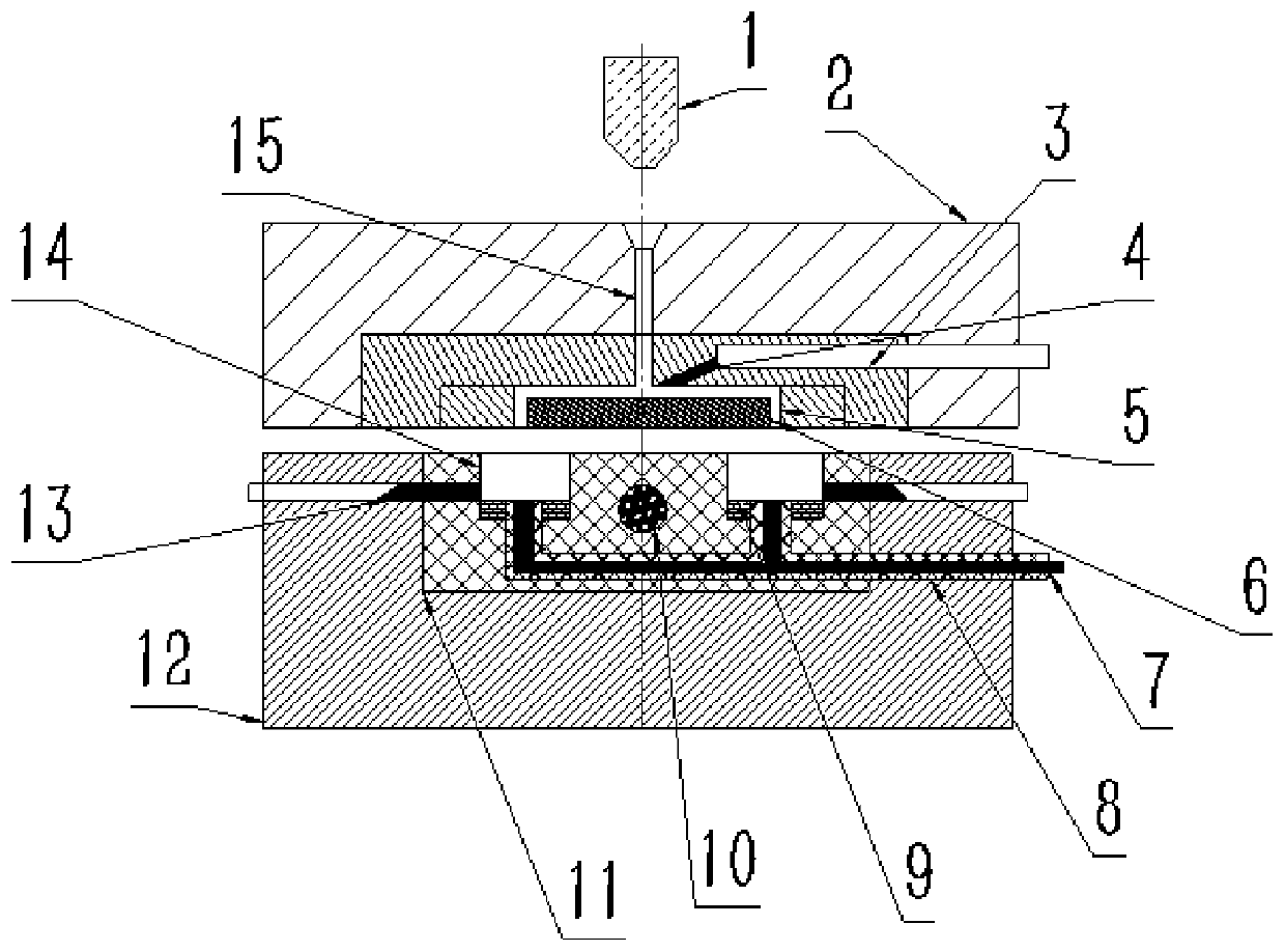
[0032] Such as figure 1 As shown, the application proposes a non-remelting high-temperature and high-pressure injection mold for power semiconductor device packaging, including a moving mold part and a fixed mold part.

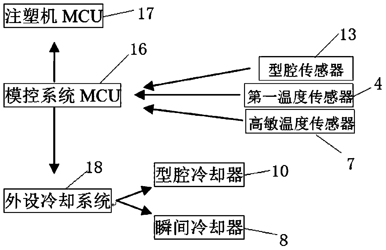
[0033] The moving mold part includes an upper mold plate 2, a hot runner plate 3 and a temperature regulating plate 6 arranged in sequence. The movable mold part is provided with a main channel 15 that runs through the upper template 2 and the hot runner plate 3, and the main channel 15 is connected with the injection nozzle 11 of the thermoplastic material injection molding machine. The hot runner plate 3 is provided with a first temperature sensor 4, and the first temperature sensor 4 is connected with an external sub-millisecond response speed temperature and pressure sensing control system for signal interaction processing. Between the temperature regulating plate 6 and the hot runner plate 3 is provided a press-fit runner heat shielding layer 5 of high h...


PUM


Abstract

The invention relates to a remelting-free high-temperature high-pressure injection mold for power semiconductor device packaging. The remelting-free high-temperature high-pressure injection mold comprises a movable mold part and a fixed mold part; the movable mold part comprises an upper mold plate, a hot runner plate and a temperature adjusting plate arranged in sequence, the movable mold part isprovided with a main runner penetrating through the upper mold plate and the hot runner plate, and the hot runner plate is internally provided with a first temperature sensor; the fixed mold assemblycomprises a lower mold and a cavity mold plate arranged in the lower mold, the cavity mold plate is internally provided with a cavity, the interior of the cavity is provided with a cavity cooler, andthe side wall of the cavity is internally provided with a pressure sensor and a second temperature sensor; and the first temperature sensor, the pressure sensor and the second temperature sensor areall connected with a mold control system. compared with the prior art, the remelting-free high-temperature high-pressure injection mold cooperates with a sub-millisecond response speed temperature andpressure sensing control technology to achieve the temperature, pressure, recrystallization speed and remelting preventing system having the three-dimensional target control characteristics, and reliable packaging of a part embedded in a third-generation semiconductor chip heterostructure is achieved.

Description

technical field [0001] The invention relates to a semiconductor device thermoplastic material packaging mold, in particular to a non-remelting high-temperature and high-pressure injection mold for power semiconductor device packaging. Background technique [0002] At present, due to the upgrade of semiconductor chip materials from the first generation to the third generation of wide bandgap materials, the existing thermosetting plastic packaging materials (mainly EMC) and injection molding (transfer molding) packaging manufacturing Devices, due to the inherent limitations of materials and processes, have been unable to take advantage of the excellent characteristics of the third-generation wide-bandgap material chips with a working junction temperature above 175°C, which in turn limits the expansion of the cost-effective advantages of third-generation semiconductor devices. However, the excellent comprehensive characteristics of thermoplastic plastic packaging materials (LCP...

Claims


Application Information

Patent Timeline
Patent Type & Authority Applications(China)
IPC IPC(8): B29C45/26B29C45/78B29C45/77B29C45/76H01L21/56
CPCB29C45/26B29C45/76B29C45/77B29C45/78B29C2945/76498B29C2945/76531B29C2945/76545H01L21/565
Inventor 管安琪马明驼鲜明
Owner 芜湖鼎联电子科技有限公司
Why Eureka
Try Eureka