Display circuit and display device

A technology for displaying circuits and sub-circuits, applied to static indicators, instruments, etc., which can solve problems such as contrast drop

Pending Publication Date: 2020-08-18
CHONGQING KONKA PHOTOELECTRIC TECH RES INST CO LTD
View PDF0 Cites 0 Cited by
  • Summary
  • Abstract
  • Description
  • Claims
  • Application Information

AI Technical Summary

Problems solved by technology

[0004] In view of the above-mentioned deficiencies in the prior art, the purpose of the present invention is to provide a display circuit and a display device to solve the problem of the non-ideal effect of the signa

Method used


Image

  • Display circuit and display device
  • Display circuit and display device
  • Display circuit and display device

Examples


Embodiment Construction

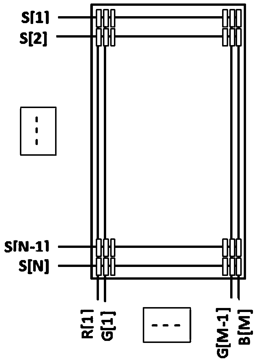
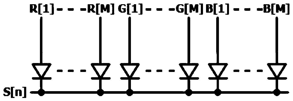
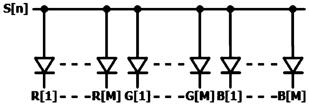
[0033] Thin Film Transistor (TFT) backplane substrate, usually using low temperature polysilicon technology (Low Temperature Poly-silicon, LTPS) or metal oxide (Metal Oxide) similar to formable rigid glass (Rigid Glass) or flexible The active device process on the polyimide (Flexible Polyimide) is manufactured, and the use of this device can create a functional circuit for the display itself to improve its additional feature advantages. Because the common electrode structure used by EL devices for light emission is used as the base element, it has not shown its greatest advantages in display products based on thin film field effect transistor (Thin Film Transistor, TFT) backplanes, especially for excellent optical specifications. required reliability capability. Therefore, the present invention provides a display circuit and a display device, and by arranging TFTs on the cathode and anode of the EL device and initializing the EL device, the purpose of high contrast ratio of th...


PUM


Abstract

The invention discloses a display circuit and a display device. The display circuit comprises a plurality of micro devices connected in a common anode or common cathode mode, wherein cathodes of the micro devices are connected with a first transistor; anodes of the micro devices are connected with a second transistor; the first transistor and the second transistor are matched to generate a reversebias voltage so as to initialize the micro devices. According to the invention, the cathodes and the anodes of the micro devices connected in a common anode or common cathode mode are respectively connected with the first transistor and the second transistor, the first transistor and the second transistor are matched to generate the reverse bias voltage to initialize the micro devices, residual charges in a previous operation time sequence are eliminated under the condition that a new time sequence needing to be operated to emit light, and background brightness generated by the residual charges is avoided, so that the low-brightness quality is improved, and the contrast ratio is increased.

Description

technical field [0001] The present invention relates to the field of display technology, in particular to a display circuit and a display device. Background technique [0002] Electroluminescence (EL) devices include organic light-emitting diodes (Organic Light-Emitting Diode, OLED), light-emitting diodes (Light-Emitting Diode, LED) and other devices. In recent years, EL devices have been widely used in the production of display products. Compared with traditional cathode ray tube displays (Cathode Ray Tube, CRT), liquid crystal displays (Liquid Crystal Display, LCD), etc., the application surface of EL devices shows better optical characteristics. Lower power consumption performance and better product shape plasticity. The common electrode structure adopted by EL devices provides important driving environment elements for the most basic display, and the most basic display is combined with the common electrode structure to extend the development of power saving (Power Savin...

Claims


Application Information

Patent Timeline
IPC IPC(8): G09G3/32G09G3/3225
CPCG09G3/32G09G3/3225H10K59/131
Inventor 郑士嵩
Owner CHONGQING KONKA PHOTOELECTRIC TECH RES INST CO LTD
Why Eureka
Try Eureka