Silicon wafer texturing post-processing method
A silicon wafer and post-cleaning technology, applied in the directions of post-processing details, post-processing, chemical instruments and methods, etc., can solve the problems of the influence of amorphous silicon deposition, organic residues, and inability to hydrophobicize the surface of silicon wafers, and achieve Isc improvement, The effect of high battery efficiency
- Summary
- Abstract
- Description
- Claims
- Application Information
AI Technical Summary
Problems solved by technology
Method used
Image


Examples
Embodiment 1
[0018] Post-processing the textured silicon wafer:
[0019] S1. Clean the silicon wafers after texturing with SC1 cleaning solution. After the final cleaning, wash off the SC1 cleaning solution on the surface of the silicon wafer with pure water. The SC1 cleaning solution is KOH and H 2 o 2 A mixed solution in which the volume fraction of 45wt% KOH is 1.6%, and the concentration is 30wt% H 2 o 2 The volume fraction is 10%, the rest is water, the temperature is 60°C, and the time is 5min;
[0020] S2, putting the silicon chip obtained in S1 into the ozone solution, at room temperature for 180s, O 3 Concentration 10ppm;
[0021] S3. Put the silicon chip obtained in S2 into the hydrofluoric acid solution for 120 seconds, and the volume fraction of HF (concentration: 49 wt%) is 10%. After the HF acid cleaning is completed, wash off the residual HF acid on the surface of the silicon chip with pure water.
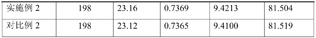
Embodiment 2
[0029] Post-processing the textured silicon wafer:
[0030] S1. Clean the silicon wafers after texturing with SC1 cleaning solution. After the final cleaning, wash off the SC1 cleaning solution on the surface of the silicon wafer with pure water. The SC1 cleaning solution is KOH and H 2 o 2 A mixed solution in which the volume fraction of 45wt% KOH is 1.6%, and the concentration is 30wt% H 2 o 2 The volume fraction is 10%, the rest is water, the temperature is 60°C, and the time is 5min;
[0031] S2. Perform chemical polishing on the silicon wafer obtained in S1. The chemical polishing liquid is a mixture of hydrofluoric acid and nitric acid, wherein the volume fraction of hydrofluoric acid with a concentration of 49 wt% is 0.5%, and the volume fraction of nitric acid with a concentration of 69 wt% is 99.5%. , the temperature is room temperature, and the time is 5min; the obtained silicon wafer is washed with pure water for 120s;
[0032] S3, putting the silicon chip obtai...
Embodiment 3
[0045] Post-processing the textured silicon wafer:
[0046] S1. Clean the silicon wafers after texturing with SC1 cleaning solution. After the final cleaning, wash off the SC1 cleaning solution on the surface of the silicon wafer with pure water. The SC1 cleaning solution is KOH and H 2 o 2 A mixed solution in which the volume fraction of 45wt% KOH is 1.6%, and the concentration is 30wt% H 2 o 2 The volume fraction is 10%, the rest is water, the temperature is 60°C, and the time is 5min;
[0047] S2. Perform chemical polishing on the silicon wafer obtained in S1. The chemical polishing liquid is a mixture of hydrofluoric acid and nitric acid, wherein the volume fraction of hydrofluoric acid with a concentration of 49 wt% is 0.5%, and the volume fraction of nitric acid with a concentration of 69 wt% is 99.5%. , the temperature is room temperature, and the time is 5min; the obtained silicon wafer is washed with pure water for 120s;
[0048] S3, putting the silicon wafer obtain...
PUM
 Abstract
Description
Claims
Application Information