Preparation method of beam lead for gan device or circuit on sic substrate

A beam-type lead and beam-type lead technology, which are applied in semiconductor/solid-state device manufacturing, circuits, semiconductor devices, etc., can solve the problems of increasing contact risk, polluting the environment, increasing costs, etc., to reduce contact risk and reduce environmental pollution , the effect of reducing the preparation cost

Active Publication Date: 2021-09-03
THE 13TH RES INST OF CHINA ELECTRONICS TECH GRP CORP
View PDF10 Cites 0 Cited by
  • Summary
  • Abstract
  • Description
  • Claims
  • Application Information

AI Technical Summary

Problems solved by technology

[0003] In view of this, an embodiment of the present invention provides a beam-type lead preparation method for a GaN device or circuit on a SiC substrate, aiming at solving the problem of metal damage, increased cost, increased contact risk and pollution caused by slicing in the prior art environmental problems

Method used


Image

  • Preparation method of beam lead for gan device or circuit on sic substrate
  • Preparation method of beam lead for gan device or circuit on sic substrate
  • Preparation method of beam lead for gan device or circuit on sic substrate

Examples


Embodiment Construction

[0032] In the following description, specific details such as specific system structures, techniques such as specific system structures, such as specific system structures are presented in order to illustrate, in order to thorns the embodiments of the present invention. However, those skilled in the art will appreciate that the present invention may be implemented in other embodiments without these specific details. In other cases, detailed description of well-known systems, devices, circuits, and methods is omitted to prevent unnecessary details to prevent the description of the present invention.

[0033] In order to illustrate the technical solution of the present invention, the following will be described below.

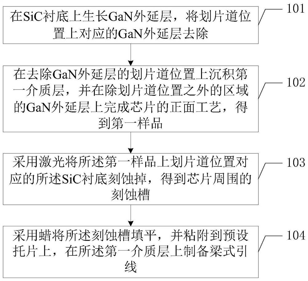
[0034] figure 1 The implementation flow of the beam lead preparation method of the GaN device or circuit is provided in the embodiment of the present invention, and is described in detail.

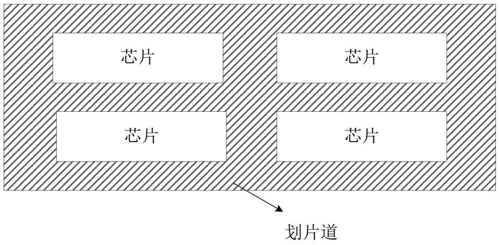
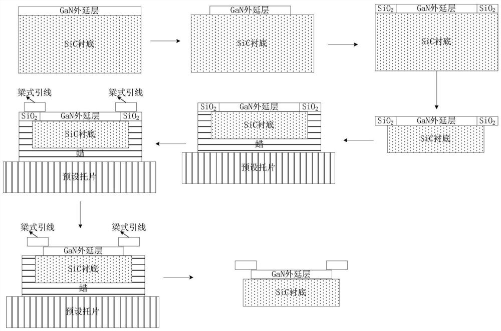
[0035] Step 101, growing the GaN epitaxial layer on the SiC substrate, remo...


PUM

PropertyMeasurementUnit
wavelengthaaaaaaaaaa

Abstract

The present invention is applicable to the technical field of semiconductor device preparation, and provides a method for preparing a beam lead of a GaN device or circuit on a SiC substrate. The method includes: growing a GaN epitaxial layer on the SiC substrate; Removal of the GaN epitaxial layer; deposit the first dielectric layer on the scribing line where the GaN epitaxial layer is removed, and complete the front-side process of the chip on the GaN epitaxial layer in the area other than the scribing line to obtain the first sample; use laser Etch the SiC substrate corresponding to the position of the scribing lane on the first sample to obtain the etching groove around the chip; fill the etching groove with wax, and adhere to the preset support, on the first dielectric layer The beam-type lead is prepared, the preparation process is simple, the device consistency is high, and the use of expensive photoresist for backfilling is avoided, so that the preparation cost of the chip is reduced, environmental pollution is reduced, and the contact risk of workers is reduced.

Description

Technical field [0001] The present invention belongs to the semiconductor device preparation technology, and in particular, the present invention relates to a beam-type lead preparation method of a GaN device or circuit on a SiC substrate. Background technique [0002] In the circuit of the operating frequency over 100GHz, a semiconductor device or circuit with a beam lead structure is widely used, and the beam lead can make the system design more compact, flexible and reliable. Currently, the traditional GaAs device or the circuit's beam lead preparation method is relatively mature. However, compared to GaAs, GaN has higher banned bandwidth, higher carrier drift speed, and higher breakdown electric fields, so it is more suitable for high-frequency power amplifier circuits and multiplier circuit development. . However, when the GaN device prepared on the SiC substrate is divided into slide, the processing method of the SiC substrate is damaged to the metal, resulting in an error ...

Claims


Application Information

Patent Timeline
Patent Type & Authority Patents(China)
IPC IPC(8): H01L21/60H01L23/482
CPCH01L24/43H01L23/4822H01L2224/431
Inventor 宋旭波梁士雄吕元杰冯志红
Owner THE 13TH RES INST OF CHINA ELECTRONICS TECH GRP CORP
Why Eureka
Try Eureka