BiOCl two-dimensional material and preparation method of BiOCl photoelectric detector
A technology of photodetectors and two-dimensional materials, applied in chemical instruments and methods, circuits, electrical components, etc., can solve problems that hinder the practical application of BiOCl photodetectors, complex preparation methods, and impurities, and achieve market promotion value High, simple preparation process, low cost effect
- Summary
- Abstract
- Description
- Claims
- Application Information
AI Technical Summary
Problems solved by technology
Method used
Image


Examples
preparation example Construction
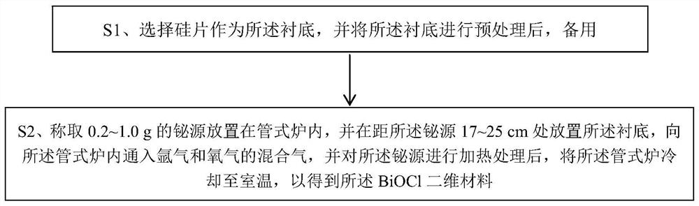
[0025] Please refer to Figure 1-2 , the embodiment of the present invention provides a method for preparing a BiOCl two-dimensional material, which mainly includes the following steps:
[0026] S1. Ultrasonic cleaning the substrate with acetone, absolute ethanol and deionized water in sequence for future use; wherein, the substrate is a silicon wafer, and after cutting the silicon wafer into a size of 10×10 mm, successively clean it with acetone, deionized water, Water ethanol and deionized water carry out ultrasonic cleaning to the described silicon chip after cutting;
[0027] S2. Select BiCl 3 As the source of bismuth, it will contain 0.2~1.0g BiCl 3 The ark is placed in the center of the tube furnace, and the ark containing the substrate is placed in the tube furnace at a position 17 to 25 cm away from the bismuth source, and a mixture of argon and oxygen is passed into the tube furnace. gas, raise the furnace temperature to 700-1000°C to heat-treat the bismuth source ...
Embodiment 1
[0029] S1, the substrate is ultrasonically cleaned with acetone, absolute ethanol and deionized water in sequence, for future use;
[0030] S2. Select BiCl 3 As the bismuth source, there will be 0.4g BiCl 3 The ark is placed in the center of the tube furnace, and an ark containing the substrate is placed at a position 18 cm away from the bismuth source in the tube furnace, and a mixture of argon and oxygen is passed into the tube furnace. The temperature of the furnace was raised to 750° C. to heat the bismuth source for 35 minutes, and then naturally cooled to room temperature to obtain a BiOCl two-dimensional material grown on the substrate.
Embodiment 2
[0032] S1, the substrate is ultrasonically cleaned with acetone, absolute ethanol and deionized water in sequence, for future use;
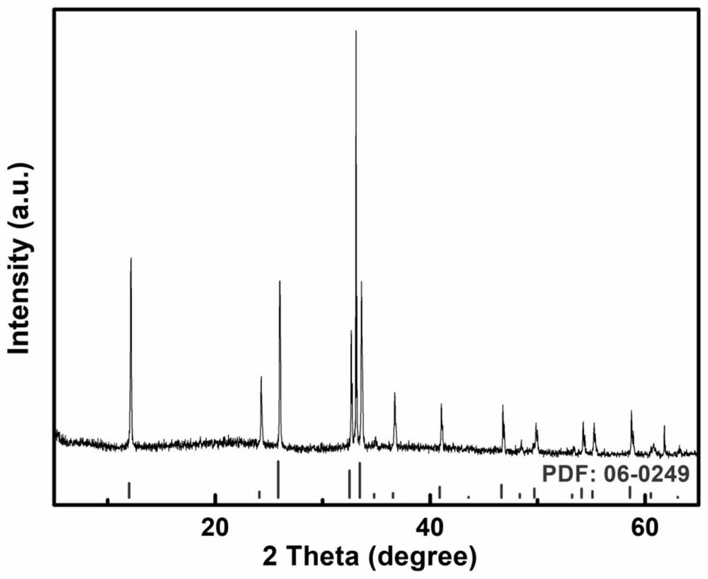
[0033] S2. Select BiCl 3 As the bismuth source, there will be 0.6g BiCl 3 The ark is placed in the center of the tube furnace, and an ark containing the substrate is placed in the tube furnace at a position 20 cm away from the bismuth source, and a mixture of argon and oxygen is passed into the tube furnace. The temperature of the furnace was raised to 800° C. to heat the bismuth source for 30 minutes, and then naturally cooled to room temperature to obtain a BiOCl two-dimensional material grown on the substrate.
[0034] The crystal structure of the BiOCl two-dimensional material obtained in this example was characterized, and the XRD test results were as follows: image 3 shown. From image 3 It can be seen that according to the PDF card NO.06-0249, the obtained BiOCl two-dimensional materials are at ~12°, ~24°, ~26°, ~32°, ~33°, ~35°, ~36°...
PUM
 Abstract
Description
Claims
Application Information
 - Generate Ideas
- Intellectual Property
- Life Sciences
- Materials
- Tech Scout
- Unparalleled Data Quality
- Higher Quality Content
- 60% Fewer Hallucinations
Browse by: Latest US Patents, China's latest patents, Technical Efficacy Thesaurus, Application Domain, Technology Topic, Popular Technical Reports.
© 2025 PatSnap. All rights reserved.Legal|Privacy policy|Modern Slavery Act Transparency Statement|Sitemap|About US| Contact US: help@patsnap.com