Raman enhancement detection method and Raman enhancement detection device for micro LED chip

A detection device and detection method technology, applied in the direction of measuring device, Raman scattering, measuring electricity, etc., can solve problems such as short circuit and leakage, and achieve the effects of reducing stray light, increasing scanning speed, and increasing the range

Active Publication Date: 2020-09-01
PEKING UNIV
View PDF10 Cites 11 Cited by
  • Summary
  • Abstract
  • Description
  • Claims
  • Application Information

AI Technical Summary

Problems solved by technology

μ-Raman can also measure the abnormal stress and carrier distribution around V-pit, void, hillock and other defects (Appl.Phys.Lett.92(21)212104( 2008), Phys.Sol.Stat.C,3(6), 2321)(2006)), these defects can lead to leakage or even short circuit

Method used


Image

  • Raman enhancement detection method and Raman enhancement detection device for micro LED chip
  • Raman enhancement detection method and Raman enhancement detection device for micro LED chip
  • Raman enhancement detection method and Raman enhancement detection device for micro LED chip

Examples


Embodiment 1

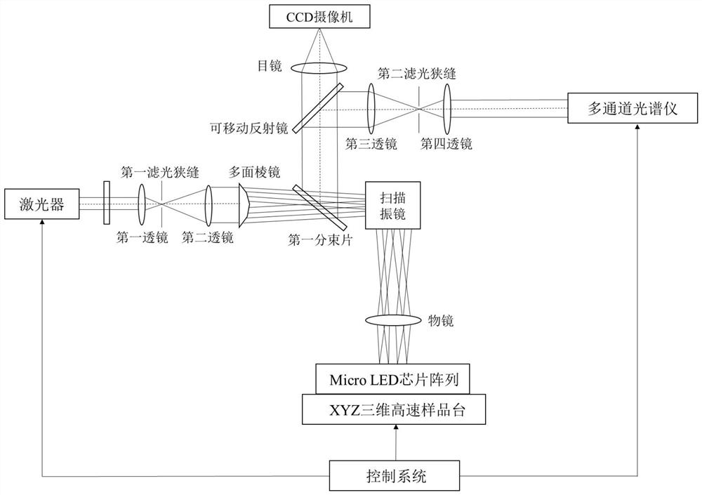
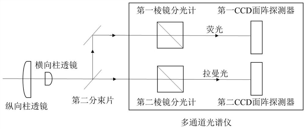
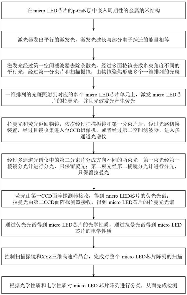
[0066] In this embodiment, the test sample is a micro LED chip with flip-chip structure.

[0067] In the example of the present invention, by adjusting the laser emission wavelength of the laser and selecting a laser with a suitable excitation wavelength, the laser photon energy is equal to or similar to the energy of some electronic transitions, and resonance is generated to enhance the Raman signal of the micro LED chip. The main detection objects of Micro LED chips are GaN and InGaN materials. For the E2, A1 (LO) and LOPC Stokes peaks of GaN materials, E2 and A1 are irreducible signs of phonon vibration, and lasers of 325-345nm are used. For the anti-Stokes Raman peak of GaN material, the excitation light wavelength is less than 350nm, so the collected Raman signal can be resonantly enhanced, and the interference from photoluminescence is less. For the E2 and A1 (LO) peaks of the InGaN material, the wavelength of the excitation light used is about 405-425nm to ensure that ther...

Embodiment 2

[0076] In this embodiment, the test sample is a micro LED chip with a vertical structure.

[0077] In the example of the present invention, by adjusting the laser emission wavelength of the laser and selecting a laser with a suitable excitation wavelength, the laser photon energy is equal to or similar to the energy of some electronic transitions, and resonance is generated to enhance the Raman signal of the micro LED chip. The main detection objects of Micro LED chips are GaN and InGaN materials. For the E2, A1 (LO) and LOPC Stokes peaks of GaN materials, the laser wavelength of 325-345nm is used, while for GaN materials, the anti-Stokes pull Mann peak, the excitation light wavelength is less than 350nm, so the collected Raman signal can be resonantly enhanced, and at the same time the interference from photoluminescence is small. For the E2 and A1 (LO) peaks of the InGaN material, the wavelength of the excitation light used is about 405-425nm to ensure that there is no strong p...


PUM

PropertyMeasurementUnit
wavelengthaaaaaaaaaa
thicknessaaaaaaaaaa

Abstract

The invention discloses a Raman enhancement detection method and a Raman enhancement detection device for a micro LED chip. According to the detection method provided by the invention, photoluminescence detection and Raman detection are combined, the photoluminescence detection provides luminescence wavelength and brightness information, and the Raman detection provides electrical properties, so that the problem of insufficient photoluminescence detection accuracy is solved; electron energy level resonance and surface plasmon resonance enhanced Raman technologies are adopted, so that the Ramanscattering intensity is enhanced by 103 to 108, part of the Raman scattering intensity reaches the photoluminescence intensity, and a foundation is laid for rapid measurement; the metal nanostructurenot only improves the luminous efficiency of the micro LED chip, but also can enhance Raman scattering signals by using surface plasmon, so that the detection speed is increased; microscopic Raman detection is a nondestructive testing means, the detection process is simple, the required time is short, the detection speed is high, the micro LED chip does not need to be specially treated, and the method is suitable for massive detection of the micro LED chip.

Description

Technical field [0001] The invention relates to the field of semiconductor devices, in particular to a Raman enhanced detection method of micro LED chips and a detection device thereof. Background technique [0002] Micro LED display technology refers to a display technology that uses self-luminous micron-level (under 50 microns) LEDs as light-emitting pixel units and is assembled on a drive panel to form a high-density LED array. When Micro LED is used for display, the number of chips reaches millions or even tens of millions. In the production process, it is necessary to detect the bad points in the display chip in time for removal or repair. For example, for a 4K TV display screen, 4K*2K*3=24M micro LED chips are required. The conventional detection and sorting speed is on the order of 10K / hour, and the detection and sorting time of a micro LED on a common 4-inch chip will reach 1000. More than hours, so fast and accurate detection of Micro LED display chips is an urgent prob...

Claims


Application Information

Patent Timeline
Patent Type & Authority Applications(China)
IPC IPC(8): G01N21/65G01N21/64G01R31/28
CPCG01N21/658G01N21/65G01N21/6402G01N21/64G01N21/6454G01N21/648G01N21/6489G01R31/2851G01N2021/655G01N2021/6417
Inventor 陈志忠潘祚坚焦飞张树霖康香宁陈怡帆詹景麟陈毅勇聂靖昕沈波
Owner PEKING UNIV
Why Eureka
Try Eureka