Micro-cavity electrode structure and organic light-emitting device

An electroluminescent device and electrode structure technology, which is applied in the direction of electric solid devices, electrical components, semiconductor devices, etc., can solve the problem that organic electroluminescent diodes cannot effectively improve color shift and other problems

Inactive Publication Date: 2020-09-04
WUHAN CHINA STAR OPTOELECTRONICS SEMICON DISPLAY TECH CO LTD
View PDF9 Cites 0 Cited by
  • Summary
  • Abstract
  • Description
  • Claims
  • Application Information

AI Technical Summary

Problems solved by technology

[0004] The purpose of the present invention is to provide a microcavity electrode structure and an organic electroluminescent device, which is used to solve the technical problem that the organic electroluminescent diode cannot effectively improve the color shift

Method used


Image

  • Micro-cavity electrode structure and organic light-emitting device
  • Micro-cavity electrode structure and organic light-emitting device
  • Micro-cavity electrode structure and organic light-emitting device

Examples


Embodiment 1

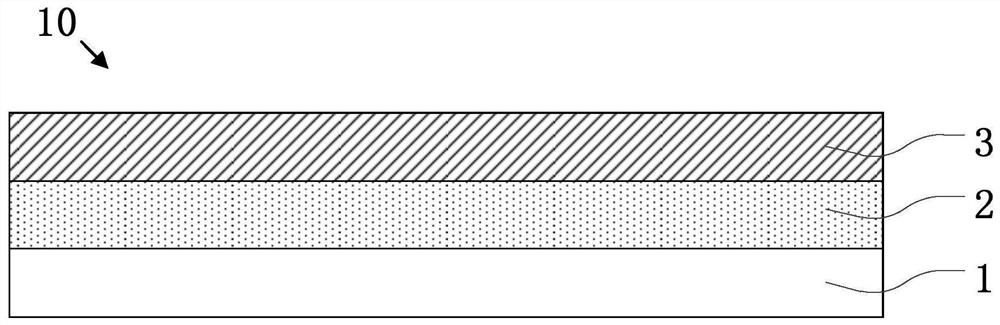
[0033] see figure 1 As shown, a microcavity electrode structure 10 is provided in the first embodiment of the present invention, including a transparent electrode layer 1, a dielectric layer 2 and a non-transparent reflective electrode layer 3; the dielectric layer 2 is arranged on the transparent electrode layer 1; the non-transparent reflective electrode layer 3 is disposed on the dielectric layer 2; wherein, the dielectric layer 2 forms a first Microcavity 110 .

[0034] In this embodiment, the optical length can be adjusted by adjusting the refractive index and thickness of the dielectric layer 2. The purpose of controlling the optical length is to achieve the highest luminous efficiency, achieve the purpose of improving luminous efficiency and control color coordinates, and realize the microcavity effect. Therefore, the dielectric layer 2 forms the first microcavity 110 .

[0035] In this embodiment, the material of the non-transparent reflective electrode layer 3 is a ...

Embodiment 2

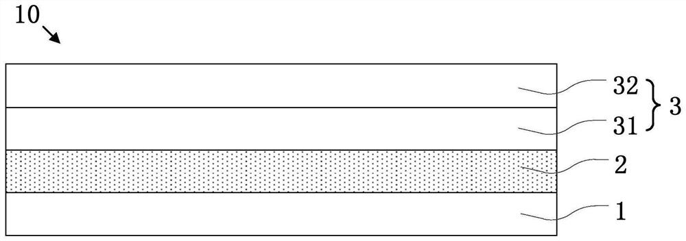
[0038] see figure 2 As shown, the second embodiment includes most of the technical features of the first embodiment, the difference is that the non-transparent reflective electrode layer 3 in the second embodiment has a two-layer structure, including a transparent conductive layer 31 and The metal reflective layer 32, instead of the non-transparent reflective electrode layer 3 in the first embodiment, has a single-layer structure.

[0039] Specifically, in this embodiment, the metal reflective layer 32 is disposed on the transparent conductive layer 31 ; the dielectric layer 2 is disposed on the metal reflective layer 32 .

[0040] In this embodiment, the material of the transparent electrode layer 1 and the transparent conductive layer 31 includes indium tin oxide; the material of the metal reflective layer 32 includes one or more alloys of Ag, Al, Mg or Ti , preferably silver.

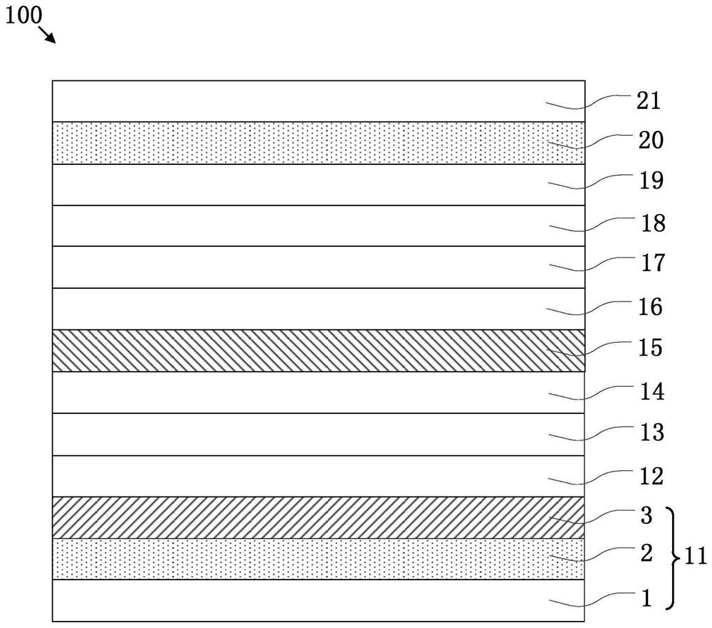
[0041] see image 3 , Figure 4As shown, an organic electroluminescent device 100 is also pr...


PUM


Abstract

The invention provides a micro-cavity electrode structure and an organic light-emitting device. The organic light-emitting device comprises the micro-cavity electrode structure, and the micro-cavity electrode structure comprises a transparent electrode layer, a dielectric layer and a non-transparent reflection electrode layer which are arranged in a stacked mode; the dielectric layer forms a firstmicro-cavity between the transparent electrode layer and the non-transparent reflective electrode layer. According to the invention, the thickness and the refractive index of the dielectric layer areregulated, so that the optical cavity length of the micro-cavity is regulated and controlled, and further color cast is overcome and the efficiency is improved; electrical property loss caused by excessive regulation of the thickness of an organic light-emitting layer is avoided; and the introduced first micro-cavity can work in cooperation with an existing second micro-cavity of an original device, color cast can be overcome more effectively, and the color cast qualification efficiency is improved.

Description

technical field [0001] The invention relates to the display field, in particular to a microcavity electrode structure and an organic electroluminescent device. Background technique [0002] Organic electroluminescent diode (OLED) display mostly adopts a top-emitting device structure. As a light-emitting component of a display device, its structure is: the bottom is a non-transparent electrode, the middle is an organic layer, and the top is a transparent electrode and a light-coupling layer. After the light is emitted from the organic layer, it is affected by the wide-angle interference effect generated by the structure from the non-transparent electrode to the transparent electrode. Adjusting the reflectivity of the electrode, the refractive index and thickness of the organic material of each layer can control the intensity and color of the outgoing light. To achieve the purpose of improving the luminous efficiency and regulating the color coordinates, this regulation is usu...

Claims


Application Information

Patent Timeline
IPC IPC(8): H01L51/52
CPCH10K50/805H10K50/852H10K50/858
Inventor 丁可
Owner WUHAN CHINA STAR OPTOELECTRONICS SEMICON DISPLAY TECH CO LTD
Why Eureka
Try Eureka