Semiconductor element processing method and forming process

A processing method and semiconductor technology, applied in semiconductor/solid-state device manufacturing, electrical components, metal processing equipment, etc., can solve the problem of easy oxidation of the surface of semiconductor chips

Inactive Publication Date: 2020-09-08
安徽富信半导体科技有限公司
View PDF9 Cites 1 Cited by
  • Summary
  • Abstract
  • Description
  • Claims
  • Application Information

AI Technical Summary

Problems solved by technology

[0005] In order to overcome the above-mentioned technical problems, the purpose of the present invention is to provide a semiconductor element processing method and molding process: (1) by taking the semiconductor wafer through double-sided photolithography as the processing object, the semiconductor wafer is put into the printing The fixed platform of the machine, use the printing machine to apply the solder paste on the upper surface of the semiconductor wafer, then take out the semiconductor wafer, and put it into the oven to dry, so that the solder paste layer on the upper surface of the semiconductor wafer is hardened, and then turn over the semiconductor wafer, Use a printing machine to coat the solder paste on the lower surface of the semiconductor wafer, then put the semiconductor wafer into an oven to dry, so that the solder paste layer on the lower surface of the semiconductor wafer is hardened, and the solder paste is coated on both sides to obtain a semiconductor Component semi-finished products, the semiconductor component semi-finished products are sent to the dicing equipment to cut out several small pieces, the cut small pieces are moved to the lead frame for packaging, and the packaged small pieces are tested for finished products to obtain the semiconductor components. (2) by putting the semi-finished semiconductor element into the first automatic loading an

Method used


Image

  • Semiconductor element processing method and forming process
  • Semiconductor element processing method and forming process
  • Semiconductor element processing method and forming process

Examples


Embodiment 1

[0036] see Figure 1-7 As shown, this embodiment is a method for processing a semiconductor element, the semiconductor element includes a semiconductor layer and a solder paste layer coated on the upper and lower surfaces of the semiconductor layer;

[0037] The semiconductor element is prepared by the following steps:

[0038] Step 1. Coating and forming: take the double-sided photolithographic semiconductor wafer as the processing object, put the semiconductor wafer into the fixed platform of the printing machine, use the printing machine to coat the solder paste on the upper surface of the semiconductor wafer, and then take it out Semiconductor wafer, and put it into the oven to dry, harden the solder paste layer on the upper surface of the semiconductor wafer, then turn over the semiconductor wafer, use a printing machine to coat the solder paste on the lower surface of the semiconductor wafer, and then semiconductor wafer, and Dry in an oven to harden the solder paste la...

Embodiment 2

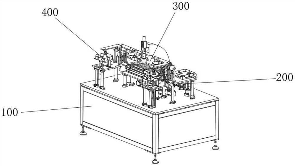
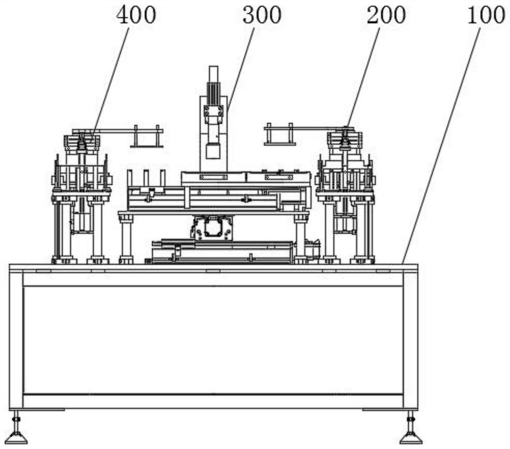
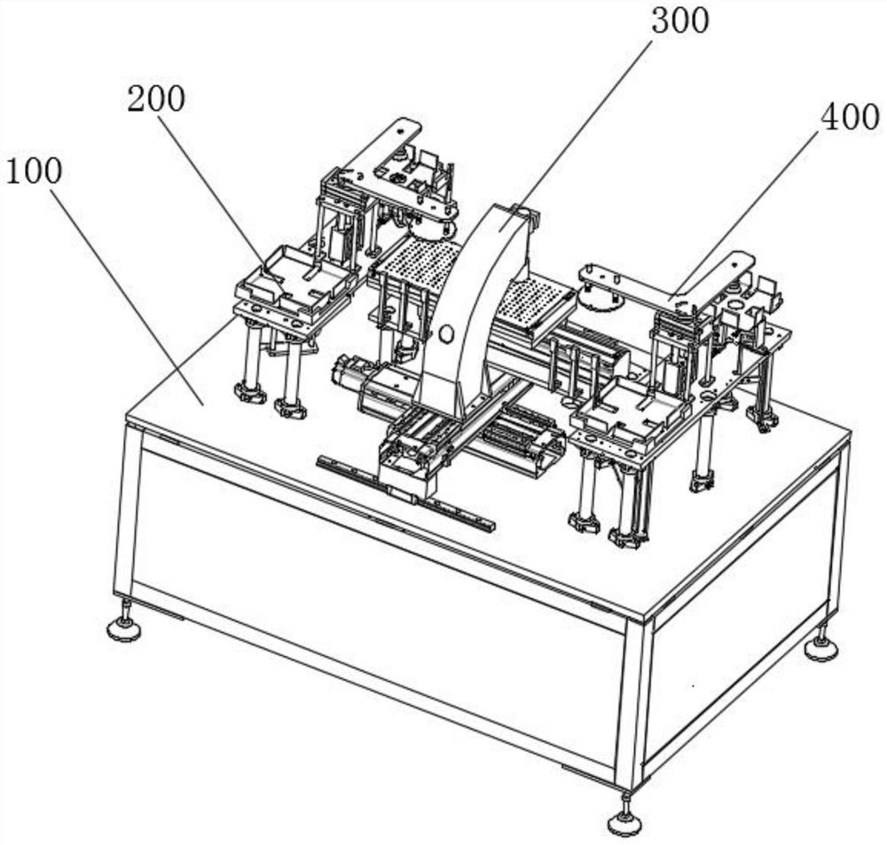
[0046] see Figure 1-7 As shown, the scribing equipment in this embodiment includes a load-bearing base 100, a first automatic loading and unloading mechanism 200, a scribing mechanism 300, and a second automatic loading and unloading mechanism 400. The top end of the load-bearing base 100 is equipped with a first automatic Loading and unloading mechanism 200, the end of the load-bearing base 100 away from the first automatic loading and unloading mechanism 200 is equipped with a second automatic loading and unloading mechanism 400, and the load-bearing base 100 is installed between the first automatic loading and unloading mechanism 200 and the second automatic loading and unloading mechanism 400 A scribing mechanism 300 is installed between them;

[0047] Wherein, the scribing mechanism 300 includes a high-energy laser generator 301, a C-shaped mounting frame 302, a first slide rail 305, a second slide rail 306, a third slide rail 311, and a dicing plate 312. The C-shaped mo...


PUM

PropertyMeasurementUnit
Thicknessaaaaaaaaaa

Abstract

The invention discloses a semiconductor element processing method and a forming process. The method comprises the steps of taking a semiconductor wafer subjected to double-sided photoetching as a processing object; coating the upper surface and the lower surface of the semiconductor wafer with soldering paste, completing double-sided coating of the soldering paste to obtain a semi-finished productof the semiconductor element, feeding the semi-finished product of the semiconductor element into scribing equipment, cutting the semi-finished product of the semiconductor element into a plurality of small blocks, moving the cut small blocks to a lead frame for packaging, and performing finished product testing on the packaged small blocks to obtain the semiconductor element. The semiconductor element processing method is simple and feasible in process, good in solder paste layer coating and fixing effect, capable of effectively preventing the surface of the semiconductor chip from being oxidized, capable of improving the compactness of the surface of the semiconductor chip and high in reliability. According to the forming process, the scribing equipment is used for preparing the semiconductor element, the scribing equipment is high in automation degree and high in feeding and discharging speed, and the production efficiency of the semiconductor element is effectively improved.

Description

technical field [0001] The invention relates to the field of semiconductor elements, in particular to a semiconductor element processing method and molding process. Background technique [0002] Semiconductors refer to materials whose conductivity is between conductors and insulators at room temperature. Semiconductors are used in integrated circuits, consumer electronics, communication systems, photovoltaic power generation, lighting, high-power power conversion and other fields. From a perspective, the importance of semiconductors is huge. Most of the chips in electronic products, such as computers, mobile phones or digital recorders, are components made of semiconductors. [0003] The surface of the existing semiconductor chip does not have a solder paste layer, and it needs to be welded together with the lead frame through the soldering sheet. However, the surface of the semiconductor chip without the solder paste layer on the surface is easy to oxidize, and even has a c...

Claims


Application Information

Patent Timeline
IPC IPC(8): H01L21/50H01L21/78B23K26/38B23K26/08B23K26/402
CPCB23K26/0876B23K26/38B23K26/402B23K2103/56H01L21/50H01L21/78
Inventor 蒋振荣周海生
Owner 安徽富信半导体科技有限公司
Why Eureka
Try Eureka