Dicing die bonding film

A chip bonding film, cutting chip technology, applied in the direction of film/sheet adhesive, adhesive type, adhesive additive, etc.

Pending Publication Date: 2020-09-11
NITTO DENKO CORP
View PDF10 Cites 0 Cited by
  • Summary
  • Abstract
  • Description
  • Claims
  • Application Information

AI Technical Summary

Problems solved by technology

The thinner the semiconductor wafer to be diced, the easier it is for cracks and defects to occur

Method used


Image

  • Dicing die bonding film
  • Dicing die bonding film
  • Dicing die bonding film

Examples


Embodiment 1

[0150]

[0151] In a reaction vessel equipped with a condenser tube, a nitrogen introduction tube, a thermometer, and a stirring device, 100 molar parts of 2-ethylhexyl acrylate (2EHA) and 21 molar parts of 2-hydroxyethyl acrylate (HEA) were used as polymerization A mixture of benzoyl peroxide as an initiator and toluene as a polymerization solvent was stirred at 60° C. for 10 hours under a nitrogen atmosphere (polymerization reaction). In this mixture, the content of benzoyl peroxide was 0.4 parts by mass with respect to 100 parts by mass of monomer components (2EHA, HEA), and the content of toluene was 80 parts by mass with respect to 100 parts by mass of monomer components. Through this polymerization reaction, an acrylic polymer containing P 1 polymer solution. For acrylic polymer P 1 The glass transition temperature (Tg) calculated based on the FoX formula was -60.6°C. Next, in the acrylic polymer containing P 1 After adding 18 mole parts of 2-methacryloyloxyethyl i...

Embodiment 2

[0157]

[0158] In a reaction vessel equipped with a condenser tube, a nitrogen introduction tube, a thermometer, and a stirring device, 75 molar parts of 2-ethylhexyl acrylate (2EHA), 25 molar parts of 4-acryloylmorpholine (ACMO), 2 A mixture of 22 mole parts of hydroxyethyl ester (HEA), benzoyl peroxide as a polymerization initiator, and toluene as a polymerization solvent was stirred at 60° C. for 10 hours under a nitrogen atmosphere (polymerization reaction). In this mixture, the content of benzoyl peroxide was 0.4 parts by mass relative to 100 parts by mass of monomer components (2EHA, ACMO, HEA), and the content of toluene was 80 parts by mass relative to 100 parts by mass of monomer components. Through this polymerization reaction, an acrylic polymer containing P 3 polymer solution. For acrylic polymer P 3 The glass transition temperature (Tg) calculated based on the FoX formula was -42.7°C. Next, in the acrylic polymer containing P 3 After adding 18 mole parts of...

Embodiment 3

[0164] The HEA used in the formation of the dicing tape adhesive layer was set to 20 mole parts instead of 21 mole parts, and instead of the base material S 1 And use the substrate S made of EVA 2 (Brand name "RB0104", thickness 125 micrometers, the Kurabo Bosho Co., Ltd. make) Except that, it carried out similarly to the dicing tape of Example 1, and produced the dicing tape of Example 3. Then, except having used this dicing tape instead of the dicing tape of Example 1, it carried out similarly to the dicing die-bonding film of Example 1, and produced the dicing die-bonding film of Example 3.


PUM

PropertyMeasurementUnit
Glass transition temperatureaaaaaaaaaa
Thicknessaaaaaaaaaa

Abstract

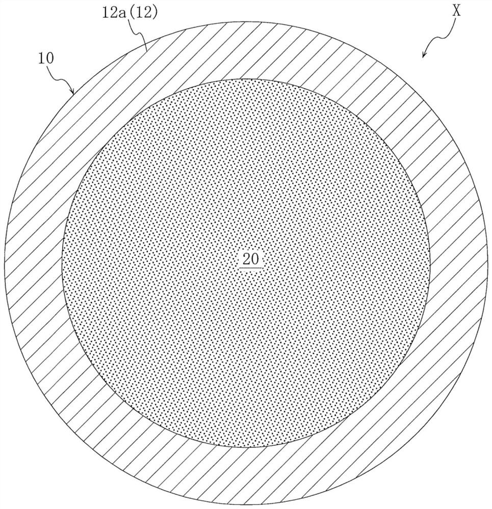
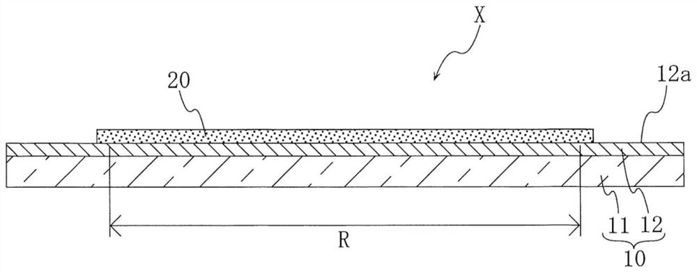
A dicing die bonding film suitable for performing an expanding process for obtaining a semiconductor chip with an adhesive layer under low temperature conditions is provided. The dicing die bonding film X of the present invention has a lamination structure including a dicing tape 10 and a die bonding film 20. The surface of the dicing tape 10 on the side of the pressure-sensitive adhesive layer 12was 0.3 N / 20 mm shows the above peel adhesion in a peel test under conditions of -15 DEG C, a peel angle of 180 DEG, and a peel rate of 300 mm / min with respect to the SUS plane. The die bonding film20 is in close contact with the pressure-sensitive adhesive layer 12 of the dicing tape 10 so as to be peelable.

Description

technical field [0001] The present invention relates to a dicing die-bonding film usable in the manufacturing process of a semiconductor device. Background technique [0002] In the manufacturing process of a semiconductor device, a dicing die-bonding film is sometimes used to obtain a semiconductor chip with an adhesive film having a size equivalent to the chip for die-bonding, that is, a semiconductor chip with an adhesive layer. A dicing die-bonding film has, for example: a dicing tape including a base material and an adhesive layer; and a die-bonding film adhered to the adhesive layer side in a peelable manner. The die-bonding film has a disk shape exceeding the size of a semiconductor wafer as a workpiece, and, for example, a dicing tape having a disk shape exceeding the size of the die-bonding film is bonded concentrically to the adhesive layer side thereof. A ring frame may be attached to an area around the die-bonding film not covered by the die-bonding film in the ...

Claims


Application Information

Patent Timeline
IPC IPC(8): C09J7/24C09J7/29C09J7/30C09J133/08C09J11/04C09J11/08H01L21/683
CPCC09J7/243C09J7/29C09J7/30C09J133/066C09J11/04C09J11/08H01L21/6836C09J2203/326C09J2433/00C09J2467/005C09J2423/046C09J2423/106H01L2221/68327H01L2221/68336C08L63/00C08L61/06C08K7/18H01L2224/73265H01L2924/181H01L2224/92247H01L2224/83191H01L2924/00012C09J7/22C09J133/04C09J11/06C09J2301/312
Inventor 木村雄大杉村敏正大西谦司宍户雄一郎福井章洋高本尚英
Owner NITTO DENKO CORP
Why Eureka
Try Eureka