Flexible touch display screen
A flexible touch and display technology, applied in the direction of instruments, electrical digital data processing, electrical components, etc., can solve the problems of product thickness limitation, complex production process, high cost, etc., to increase the performance of bending resistance and expand the application scene , the effect of preventing short circuit problems
- Summary
- Abstract
- Description
- Claims
- Application Information
AI Technical Summary
Problems solved by technology
Method used
Image
Examples
Embodiment 1
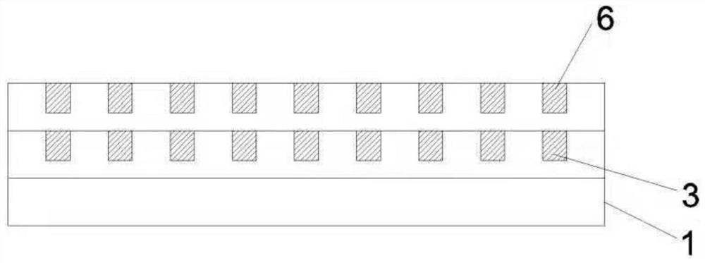
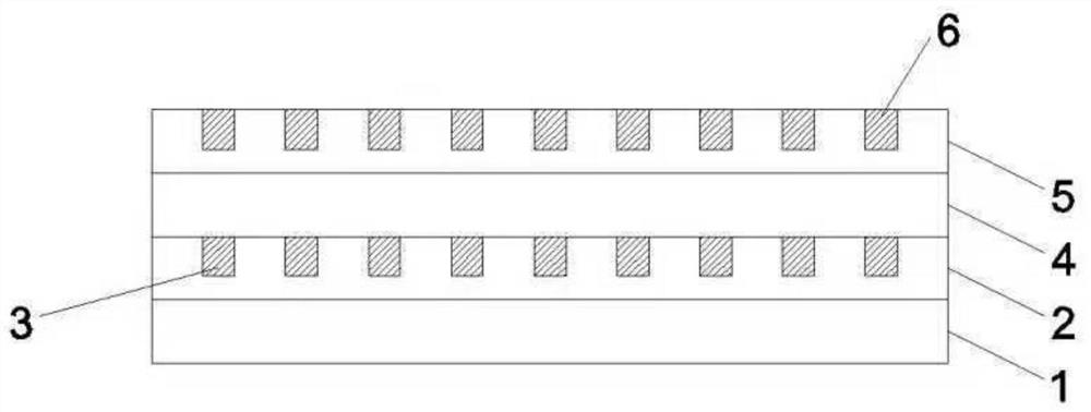
[0051] Such as figure 1 As shown, the present embodiment discloses a touch conductive film for a flexible touch display screen, which includes a transparent substrate 1, on which a first UV glue layer 2 is provided, and the first conductive layer 3 is formed by a pattern The conductive material is embossed on the first UV adhesive layer 2 in a plurality of grid grooves; the transparent reinforced insulating support layer 4 is provided with a third UV adhesive layer 5, and the second conductive layer 6 is composed of The pattern embossed on the third UV adhesive layer 5 is composed of conductive materials in a plurality of grid grooves.
[0052] It should be noted that the third UV adhesive layer containing the second conductive layer is arranged on the second UV adhesive layer (reinforced insulating support layer) cured after imprinting, which can greatly improve the first conductive layer and the second conductive layer. Insulation strength between, to avoid the problem of cond...
Embodiment 2
[0095] Such as Figure 4 As shown, this embodiment discloses another touch conductive film for a flexible touch display screen, which includes a transparent substrate 1, a first conductive layer 3 disposed on the transparent substrate, and a second conductive layer 3 disposed on the first conductive layer. Two conductive layers 6, a transparent reinforced insulating support layer 4 is provided between the first conductive layer 3 and the second conductive layer 6, and the second conductive layer 6 is provided on the cured reinforced insulating support layer 4;
[0096] The difference from the first embodiment is that the first conductive layer of the second embodiment is formed of conductive material filled in grid grooves opened on the transparent substrate 1.
[0097] It should be noted that compared with the first embodiment, the second embodiment has the first UV glue layer removed, which is equivalent to a thinner touch conductive film, but the effect of directly imprinting the...
PUM
| Property | Measurement | Unit |
|---|---|---|
| Thickness | aaaaa | aaaaa |
| Thickness | aaaaa | aaaaa |
| Thickness | aaaaa | aaaaa |
Abstract
Description
Claims
Application Information
 - R&D
- Intellectual Property
- Life Sciences
- Materials
- Tech Scout
- Unparalleled Data Quality
- Higher Quality Content
- 60% Fewer Hallucinations
Browse by: Latest US Patents, China's latest patents, Technical Efficacy Thesaurus, Application Domain, Technology Topic, Popular Technical Reports.
© 2025 PatSnap. All rights reserved.Legal|Privacy policy|Modern Slavery Act Transparency Statement|Sitemap|About US| Contact US: help@patsnap.com


