Planarization method of MRAM device

A planarization method and device technology, applied in the manufacturing/processing of components of electromagnetic equipment, resistors controlled by magnetic fields, and electromagnetic devices, can solve the problems of uneven wafer surface and affecting the function of MRAM devices, etc., and achieve easy Effects of controlling, reducing adverse effects, and improving control capabilities

Pending Publication Date: 2020-09-22
CETHIK GRP +1
View PDF8 Cites 0 Cited by
  • Summary
  • Abstract
  • Description
  • Claims
  • Application Information

AI Technical Summary

Problems solved by technology

Due to the different selection ratios of different thin film materials, and there is no mature slurry product for TEOS / SiN / Ta on the market at the same time, therefore, in the actual CMP process, it is necessary to accurately stop the polishing end point above the magnetic tunnel junction The metal thin film protective layer is very challenging, and the surface of the wafer is often uneven, which affects the function of the MRAM device

Method used


Image

  • Planarization method of MRAM device
  • Planarization method of MRAM device
  • Planarization method of MRAM device

Examples


Embodiment Construction

[0032] In order to make the purpose, technical solutions and advantages of the embodiments of the present invention clearer, the technical solutions in the embodiments of the present invention will be clearly and completely described below in conjunction with the drawings in the embodiments of the present invention. Obviously, the described embodiments It is only some embodiments of the present invention, but not all embodiments. Based on the embodiments of the present invention, all other embodiments obtained by persons of ordinary skill in the art without making creative efforts belong to the protection scope of the present invention.

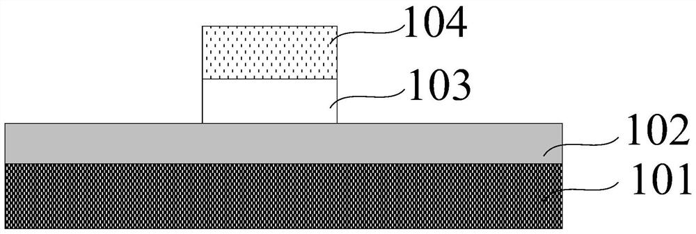
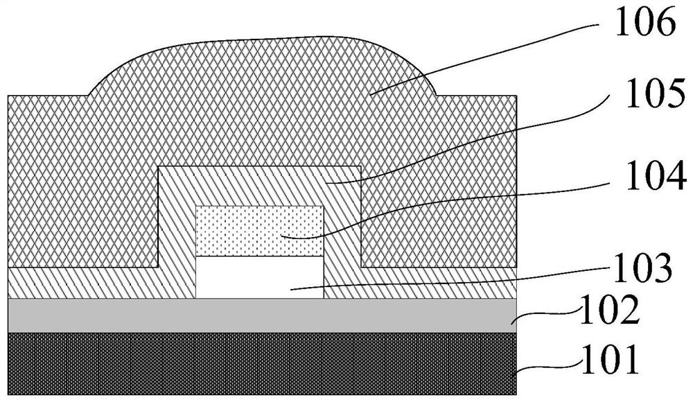
[0033] An embodiment of the present invention provides a method for planarizing an MRAM device, such as figure 1 As shown, it is the initial structure of the MRAM device that needs to be planarized. The MRAM device includes a substrate 101, and a memory cell structure is arranged on the substrate 101. The memory cell structure includes at lea...


PUM


Abstract

The invention provides a planarization method of an MRAM device. The MRAM device comprises a substrate, and the substrate is provided with a storage unit structure; the storage unit structure at leastcomprises a bottom electrode and a magnetic tunnel junction located on the bottom electrode, and the upper surface of the magnetic tunnel junction is provided with a metal film protection layer. Themethod comprises the following steps: sequentially depositing a polishing barrier layer and a dielectric layer on the substrate; chemically and mechanically polishing the dielectric layer until all the polishing barrier layers above the metal film protective layer are exposed; etching the polishing barrier layer, and removing all the polishing barrier layer on the upper surface of the metal thin film protection layer and part of the polishing barrier layer on the two sides of the metal thin film protection layer. According to the planarization method provided by the invention, the control capability of the polishing end point in the CMP process can be improved, and the electrical interconnection between the MTJ unit and the top electrode in the MRAM device is improved.

Description

technical field [0001] The invention relates to the technical field of magnetic memory, in particular to a method for planarizing an MRAM device. Background technique [0002] Magnetic Random Access Memory (MRAM) is a new type of non-volatile memory. Compared with other types of memory at present, it has fast read and write speeds, can achieve unlimited erasing and writing, and is easy to integrate with current semiconductor processes. In addition, the spin transfer torque (Spin transfer torque, STT) MRAM array using spin current to achieve magnetic moment reversal can realize the miniaturization of the memory cell size. These advantages make MRAM the main development direction of new memory in the future. [0003] The main functional unit in the MRAM device is the MTJ unit, and its structure mainly includes a magnetic free layer / nonmagnetic oxide layer (MgO) / magnetic pinning layer. Driven by an external magnetic field or current, the direction of the magnetic moment of th...

Claims


Application Information

Patent Timeline
Patent Type & Authority Applications(China)
IPC IPC(8): H01L43/12H01L43/08H01L43/02
CPCH10N50/80H10N50/10H10N50/01
Inventor 刘鲁萍王雷
Owner CETHIK GRP
Why Eureka
Try Eureka