
A kind of semiconductor mesa metal stripping method

A metal lift-off and semiconductor technology, applied in the direction of semiconductor devices, semiconductor/solid-state device manufacturing, electrical components, etc., can solve the problems of difficulty in ensuring the flatness of the photoresist, affecting the metal lift-off process, and poor film thickness uniformity, so as to avoid film thickness The effects of poor uniformity, reduced thickness requirements, and pollution avoidance

Active Publication Date: 2021-02-19
YANGZHOU GUOYU ELECTRONICS
View PDF17 Cites 0 Cited by
  • Summary
  • Abstract
  • Description
  • Claims
  • Application Information

AI Technical Summary

Problems solved by technology

[0005] The purpose of the present invention is to provide a metal stripping method for semiconductor mesas to solve the problem of manually dipping photoresist with a paintbrush and coating it on the side of the chip in the prior art, which is time-consuming and laborious, and it is difficult to ensure the smoothness of the photoresist and poor uniformity of film thickness. Technical issues that affect the subsequent metal stripping process

Method used


Image

  • A kind of semiconductor mesa metal stripping method
  • A kind of semiconductor mesa metal stripping method
  • A kind of semiconductor mesa metal stripping method

Examples


Embodiment 1

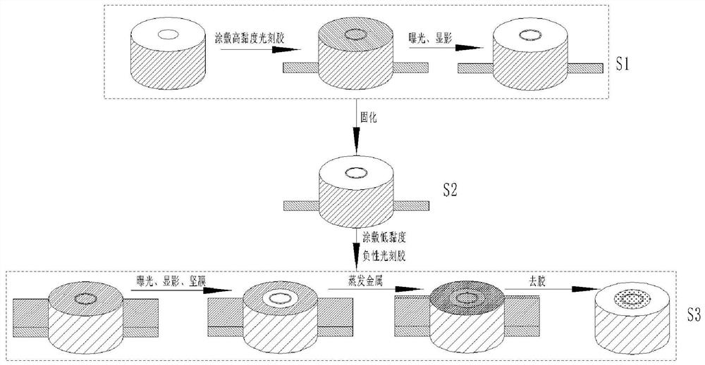
[0043] This embodiment discloses a semiconductor mesa metal stripping method, including the following steps:

[0044] S1 uses high-viscosity photoresist to apply glue to the wafer table and periphery, and then performs exposure, development, and glue removal operations in sequence to retain the high-viscosity photoresist on the periphery and the high-viscosity photoresist in the scribing lane of the table;

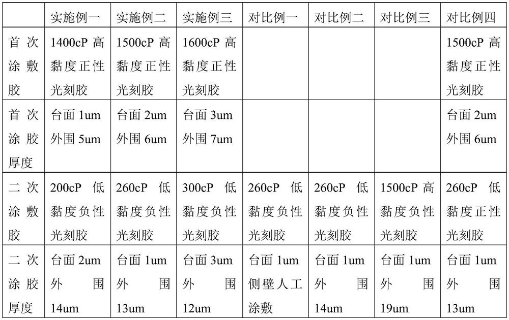
[0045] Among them, the viscosity of the high-viscosity photoresist is 1400cP, the coating thickness of the high-viscosity photoresist on the mesa is 1um, and the thickness of the peripheral coating is 5um.

[0046]The high-viscosity photoresist is a positive photoresist, and only the mesa area is exposed during the exposure process, and a mask is used to block the scribe line.

[0047] S2 heating and baking the wafer obtained in step S1 to cure the high-viscosity photoresist at a heating temperature of 140° C. for 40 minutes.

[0048] S3 uses a low-viscosity negative phot...

Embodiment 2

[0052] This embodiment discloses a semiconductor mesa metal stripping method, including the following steps:

[0053] S1 uses high-viscosity photoresist to apply glue to the wafer table and periphery, and then performs exposure, development, and glue removal operations in sequence to retain the high-viscosity photoresist on the periphery and the high-viscosity photoresist in the scribing lane of the table;

[0054] Among them, the high-viscosity photoresist is polyfiber PI positive photoresist, the specific model is PW-1500, the viscosity is 1500cP, and it has high temperature resistance. 6um.

[0055] During the exposure process, only the mesa area is exposed, and a mask is used to block the scribe lane.

[0056] S2 heating and baking the wafer obtained in step S1 to cure the high-viscosity photoresist at a heating temperature of 150° C. for 30 minutes.

[0057] S3 uses a low-viscosity negative photoresist to apply glue to the wafer table and periphery obtained in the step ...

Embodiment 3

[0061] This embodiment discloses a semiconductor mesa metal stripping method, including the following steps:

[0062] S1 uses high-viscosity photoresist to apply glue to the wafer table and periphery, and then performs exposure, development, and glue removal operations in sequence to retain the high-viscosity photoresist on the periphery and the high-viscosity photoresist in the scribing lane of the table;

[0063] Among them, the viscosity of the high-viscosity photoresist is 1600cP, which has high temperature resistance. The thickness of the high-viscosity photoresist on the table is 3um, and the thickness of the peripheral coating is 7um.

[0064] During the exposure process, only the mesa area is exposed, and a mask is used to block the scribe lane.

[0065] S2 heating and baking the wafer obtained in step S1 to cure the high-viscosity photoresist at a heating temperature of 160° C. for 20 minutes.

[0066] S3 uses a low-viscosity negative photoresist to apply glue to the...


PUM


Abstract

The invention discloses a semiconductor mesa metal stripping method which comprises the following steps: S1, gluing a wafer mesa and the periphery of the wafer mesa by adopting high-viscosity photoresist, then sequentially exposing and developing, and reserving the high-viscosity photoresist at the periphery; S2, heating and baking the wafer obtained in the step S1, and curing the high-viscosity photoresist; and S3, coating the table surface and the periphery of the wafer obtained in the step S2 with a low-viscosity negative photoresist, and then sequentially exposing, developing, hardening, evaporating metal and removing the photoresist to obtain the electrode. High-viscosity photoresist is used for gluing a table top and the periphery of a wafer, peripheral gluing is reserved through exposure and development, and the high-viscosity photoresist is cured to form a substrate. The low-viscosity negative photoresist is directly coated on the substrate, and the low-viscosity negative photoresist and the cured high-viscosity photoresist are matched to completely wrap the side wall of the wafer, so that the side wall of the wafer can be prevented from being polluted in a metal evaporation link, a glue layer is ensured to be flat and uniform, and subsequent metal stripping is facilitated.

Description

technical field [0001] The invention relates to the technical field of semiconductor manufacturing, in particular to a semiconductor mesa metal stripping method. Background technique [0002] The mesa metal lift-off method is to cover the entire mesa with photoresist as a substrate, and after exposure, the photoresist on the part not covered by the mask will undergo an exposure reaction to realize the transfer of the circuit pattern from the mask to the silicon wafer; using chemical development The liquid dissolves the soluble area of ​​the photoresist caused by exposure, so that visible patterns appear on the silicon wafer; after heat drying to remove the remaining solvent, the metal is evaporated, and then the glue is removed by ultrasonication of the glue remover, and the metal on the glue is peeled off at the same time , Retain the metal on the table to form electrodes; the stripping method can effectively solve the problem that it is not easy to prepare fine patterns by...

Claims


Application Information

Patent Timeline
Patent Type & Authority Patents(China)
IPC IPC(8): H01L21/3213H01L21/28H01L21/027G03F7/42G03F7/16
CPCG03F7/16G03F7/42H01L21/0274H01L21/28H01L21/32134
Inventor 王秋建刘智王颖
Owner YANGZHOU GUOYU ELECTRONICS
Learn More