
Phase change material structure, memory unit and manufacturing method thereof

A technology of memory cells and phase change materials, which is applied in metal material coating technology, electrical components, vacuum evaporation plating, etc., can solve the problems of easy diffusion and thermal stability of antimony, achieve excellent thermal stability, prevent diffusion, and inhibit antimony The effect of phase separation

Inactive Publication Date: 2020-09-29
SHANGHAI INST OF MICROSYSTEM & INFORMATION TECH CHINESE ACAD OF SCI
View PDF10 Cites 2 Cited by
  • Summary
  • Abstract
  • Description
  • Claims
  • Application Information

AI Technical Summary

Problems solved by technology

[0005] In order to improve the technical problems of easy diffusion of antimony (Sb) and poor thermal stability of existing phase change materials mentioned in the background technology

Method used


Image

  • Phase change material structure, memory unit and manufacturing method thereof
  • Phase change material structure, memory unit and manufacturing method thereof

Examples


Embodiment Construction

[0044] The technical solutions in the embodiments of the present application will be clearly and completely described below in conjunction with the drawings in the embodiments of the present application. Obviously, the described embodiments are only a part of the embodiments of the present application, rather than all the embodiments. Based on the embodiments in this application, all other embodiments obtained by those of ordinary skill in the art without creative work shall fall within the protection scope of this application.

[0045] The "one embodiment" or "embodiment" referred to herein refers to a specific feature, structure, or characteristic that can be included in at least one implementation of the present application. In the description of this application, it should be understood that the orientation or positional relationship indicated by the terms "upper", "lower", "top", "bottom", etc. are based on the orientation or positional relationship shown in the drawings, an...


PUM

PropertyMeasurementUnit
thicknessaaaaaaaaaa
thicknessaaaaaaaaaa
thicknessaaaaaaaaaa

Abstract

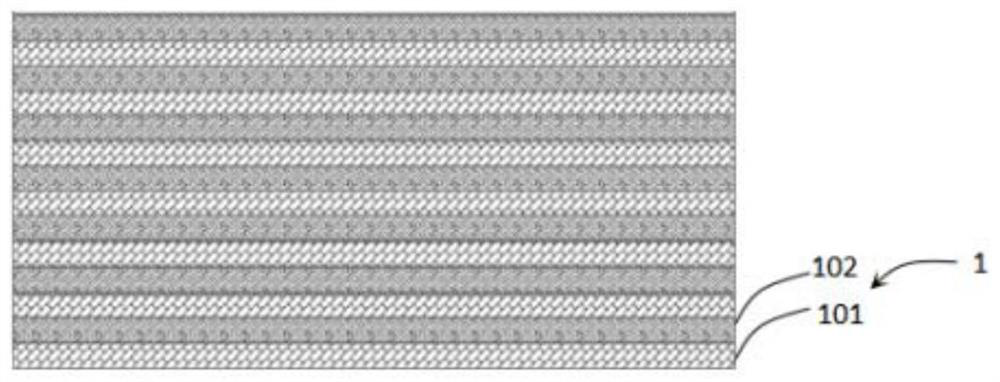
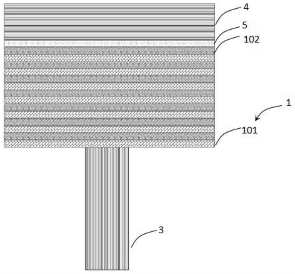
The invention relates to the technical field of micro-nano electronics, and discloses a phase change material structure, which comprises a first material layer and a second material layer, and is characterized in that the first material layer is arranged on the second material layer, wherein the material of the first material layer is a compound comprising two chemical elements of titanium (Ti) and tellurium (Te), the general chemical formula of the material of the first material layer is titanium telluride (TixTey), wherein x and y are atomic percentages of the elements; and the second material layer is made of antimony (Sb). The phase change material structure provided by the invention has the characteristics of blocking antimony (Sb) diffusion, and being good in thermal stability and high in phase change speed.

Description

Technical field [0001] The present invention relates to the technical field of micro-nano electronics, in particular to a phase change material structure, a memory unit and a manufacturing method thereof. Background technique [0002] As an important part of the integrated circuit industry, semiconductor memory currently has a variety of semiconductor storage technologies, including conventional volatile storage technologies, such as SRAM (Static Random-Access Memory) and DRAM (Dynamic Random Access). Memory, dynamic random access memory); and non-volatile storage technologies, such as EEPROM (Electrically Erasable Programmable Read Only Memory) and FLASH (flash memory). These technologies have already played a huge role in the fields of large data centers, consumer electronics and automotive electronics. However, with the development of information technology, large data centers have put forward higher requirements for storage density, power consumption, and speed. Product upgr...

Claims


Application Information

Patent Timeline
Patent Type & Authority Applications(China)
IPC IPC(8): H01L45/00C23C14/06C23C14/18C23C14/35
CPCC23C14/0623C23C14/185C23C14/352H10N70/026H10N70/8828
Inventor 宋志棠宋文雄赵进
Owner SHANGHAI INST OF MICROSYSTEM & INFORMATION TECH CHINESE ACAD OF SCI
Learn More