Semiconductor device modeling method

A device modeling and semiconductor technology, applied in instruments, special data processing applications, electrical digital data processing, etc., can solve problems such as complex formulas and slow simulation speed, and achieve simple models, elevated substrate pressure drop, and good convergence Effect

Active Publication Date: 2020-10-02
JOULWATT TECH INC LTD
View PDF30 Cites 1 Cited by
  • Summary
  • Abstract
  • Description
  • Claims
  • Application Information

AI Technical Summary

Problems solved by technology

[0006] like image 3 As shown, the conventional GGNMOS modeling method divides the whole device into native transistor T1, parasitic transistor B1, impact ionization current source I GEN and substrate resistance R sub , the lead-out terminal includes the source S, drain D, gate G of the native transistor T1 and the base B of the parasitic transistor B1, where the key focus of modeling is the impact ionization current source I GEN The impact ionization current I gen In the traditional GGNMOS modeling, the native transistor T1 (native transistor model) uses a simple MOS model, and the parasitic transistor B1 (parasitic transistor model) uses a simple EM model or GP model. Ionization current I gen Verilog-A language is usually used for representation, the formula is relatively complicated, and the simulation speed is slow

Method used


Image

  • Semiconductor device modeling method
  • Semiconductor device modeling method
  • Semiconductor device modeling method

Examples


Embodiment Construction

[0030] Various embodiments of the invention will be described in more detail below with reference to the accompanying drawings. In the various drawings, the same elements are denoted by the same or similar reference numerals. For the sake of clarity, various parts in the drawings have not been drawn to scale.

[0031] The specific implementation manners of the present invention will be further described in detail below in conjunction with the accompanying drawings and embodiments.

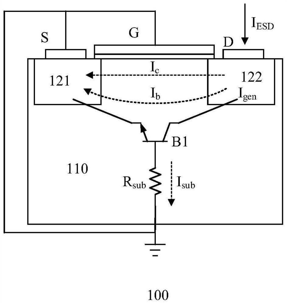
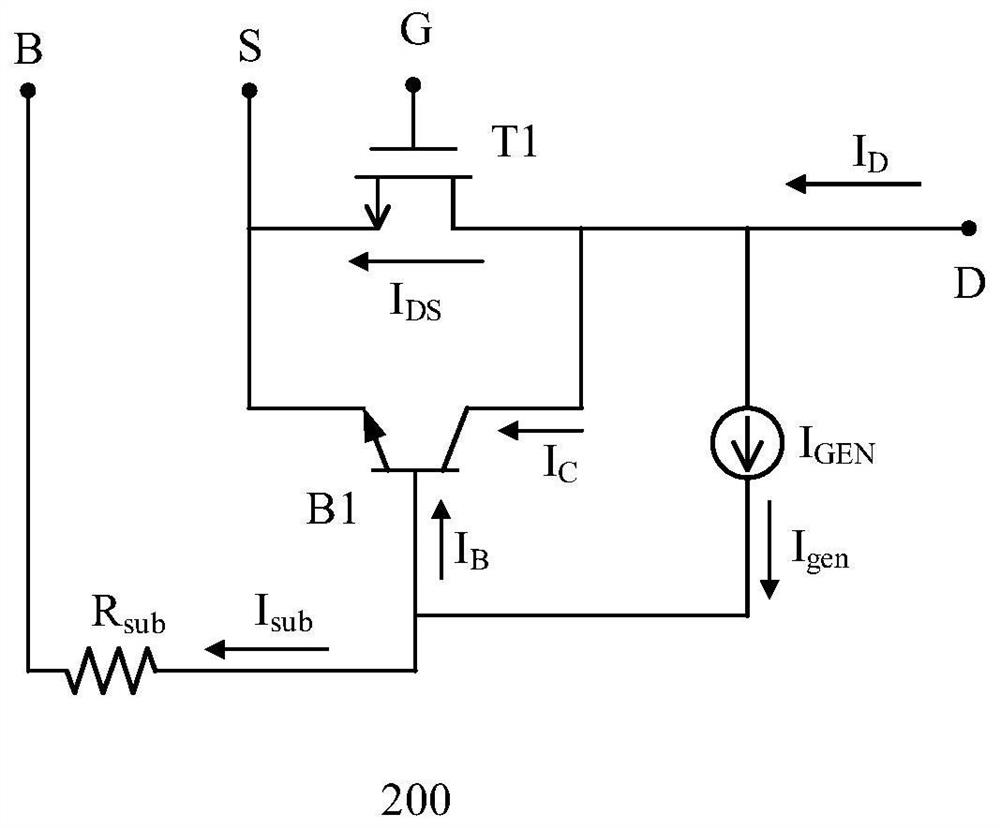
[0032] Figure 4 A schematic circuit structure diagram showing a GGNMOS model of a semiconductor device modeling method according to an embodiment of the present invention.

[0033] like Figure 4 As shown, the GGNMOS model of the embodiment of the present invention divides the whole device into native transistor T2 (native transistor model), parasitic transistor B2 (parasitic transistor model), substrate resistance R sub , source resistance R s and the drain resistor R d .

[0034] The subs...


PUM


Abstract

The invention discloses a semiconductor device modeling method which comprises the steps that a native transistor model and a parasitic transistor model are established, and a substrate of the nativetransistor model is connected to a base electrode of the parasitic transistor model and grounded through a substrate resistor; the drain electrode of the native transistor model and the collector electrode of the parasitic transistor are connected to the drain end of the semiconductor device through a drain end resistor; the source of the native transistor model and the emitter of the parasitic transistor are both connected to the source of the semiconductor device. According to the semiconductor device modeling method, a native transistor model and a parasitic transistor model respectively comprise a collision ionization current formula; by setting two collision ionization current formulas, the rise of the substrate voltage can be ensured, the starting of a parasitic transistor model is ensured, the analogue simulation of a snapback phenomenon is ensured, the parameter acquisition of the ESD device is ensured, the model is simple, the convergence is good, and the simulation speed is high.

Description

technical field [0001] The invention relates to the technical field of semiconductors, in particular to a modeling method for semiconductor devices. Background technique [0002] With the continuous progress of the technology, the thickness of the gate oxide of the device is continuously reduced, and the internal circuit of the chip is more and more vulnerable to damage caused by static electricity, and the requirements for the capability of ESD (Electro-Static discharge, electrostatic discharge) devices including circuits are also increasing. higher. Among them, the gate-grounded NMOS (N-Metal-Oxide-Semiconductor, N-type metal-oxide-semiconductor) tube (gate-grounded NMOS, GGNMOS) is the most widely used ESD device. In order to ensure the reliability of ESD, accurate Predict the protection ability of the protection circuit of GGNMOS to optimize the circuit design, reduce the design cycle and improve the reliability of the chip. SPICE (Simulation program with integrated ci...

Claims


Application Information

Patent Timeline
Patent Type & Authority Applications(China)
IPC IPC(8): G06F30/3308
CPCG06F30/3308Y02E60/00
Inventor 蒋盛烽
Owner JOULWATT TECH INC LTD
Why Eureka
Try Eureka