
Packaging structure and forming method of packaging structure

A technology of packaging structure and heat dissipation structure, applied in the direction of semiconductor/solid-state device parts, semiconductor devices, electrical components, etc., can solve the problems of affecting the welding quality of the metal solder layer, unable to form air holes, and unable to discharge flux, etc. Strength, short circuit prevention, yield improvement effect

Active Publication Date: 2020-10-02
SUZHOU TF AMD SEMICON CO LTD
View PDF6 Cites 0 Cited by
  • Summary
  • Abstract
  • Description
  • Claims
  • Application Information

AI Technical Summary

Problems solved by technology

[0002] Traditional BGA products mainly include substrates and passive components arranged on the substrates, bottom sealant, chips, and solder balls. This packaging structure has the advantage of low warpage, but the heat dissipation performance is poor. The current BGA products are mainly equipped with heat dissipation covers. And connect the heat dissipation cover and the chip through the metal solder layer (such as indium sheet) to conduct heat and improve the purpose of heat dissipation. However, the existing packaging structure puts the metal solder layer in a closed environment, so that the metal solder layer volatilizes during soldering. The flux cannot be discharged, which affects the soldering quality of the metal solder layer
[0003] In the application document with the application publication number CN110854083A, a semiconductor chip packaging structure and packaging process are disclosed, which forms a row by not setting a sealing material at the position corresponding to the air passage between the first heat dissipation structure and the first surface. Air holes, the volatilized flux is discharged through the air vents; however, this method has high requirements for the amount of sealing layer material and the mounting accuracy of the first heat dissipation structure, and it is easy to form small air holes or form no vent problem

Method used


Image

  • Packaging structure and forming method of packaging structure
  • Packaging structure and forming method of packaging structure
  • Packaging structure and forming method of packaging structure

Examples


Embodiment Construction

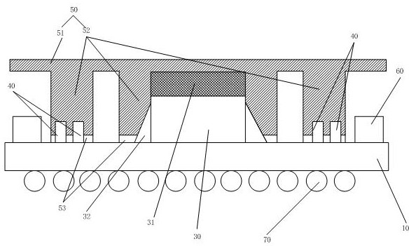
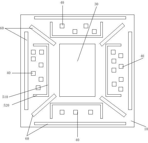
[0026] The application will be further described in detail below in conjunction with the accompanying drawings and embodiments. It should be understood that the specific embodiments described here are only used to explain related inventions, rather than to limit the invention. It should also be noted that, for ease of description, only parts related to the invention are shown in the drawings.

[0027] It should be noted that, in the case of no conflict, the embodiments in the present application and the features in the embodiments can be combined with each other. The present application will be described in detail below with reference to the accompanying drawings and embodiments.

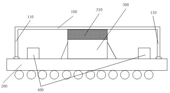
[0028] refer to figure 1 , is an existing packaging structure, heat dissipation is achieved by setting a heat dissipation cover 100 on the substrate 200, and the heat dissipation cover is connected to the heat dissipation cover 100 through a metal solder layer 310 to transfer heat, because the sub...


PUM


Abstract

The invention discloses a packaging structure and a forming method of the packaging structure. According to the invention, the packaging structure comprises a heat dissipation structure, wherein the first heat dissipation part of the heat dissipation structure can separate a solder layer from a passive element, so that the risk of short circuit caused by the fact that metal solder splashes to thepassive element during solder layer welding is avoided; the first heat dissipation part is located in the area close to the center of the substrate, so that the influence of warping of the substrate on the welding layer can be reduced so as to avoid the breakage of the solder layer structure; the multiple first heat dissipation parts are arranged at intervals, and when reflux soldering is conducted on the solder layer, volatilized soldering flux can be discharged from gaps between the first heat dissipation parts, so that the soldering quality of the solder layer is guaranteed, and the strength of the solder layer is guaranteed; and according to the packaging structure and the forming method of the packaging structure, the reliability of the product can be improved, and the yield of the product is improved.

Description

technical field [0001] The present invention generally relates to the field of semiconductor manufacturing, and in particular to a packaging structure and a method for forming the packaging structure. Background technique [0002] Traditional BGA products mainly include substrates and passive components arranged on the substrates, bottom sealant, chips, and solder balls. This packaging structure has the advantage of low warpage, but the heat dissipation performance is poor. The current BGA products are mainly equipped with heat dissipation covers. And connect the heat dissipation cover and the chip through the metal solder layer (such as indium sheet) to conduct heat and improve the purpose of heat dissipation. However, the existing packaging structure puts the metal solder layer in a closed environment, so that the metal solder layer volatilizes during soldering. The flux cannot be discharged, which affects the soldering quality of the metal solder layer. [0003] The appl...

Claims


Application Information

Patent Timeline
Patent Type & Authority Applications(China)
IPC IPC(8): H01L23/367H01L25/16H01L23/24H01L21/50
CPCH01L21/50H01L23/24H01L23/367H01L25/16
Inventor 卢玉溪马晓波王金惠
Owner SUZHOU TF AMD SEMICON CO LTD
Learn More