Film coating equipment, method and system, solar cell, assembly and power generation system

A technology for solar cells and solar cells, applied in photovoltaic power generation, electrical components, circuits, etc., can solve problems such as low processing efficiency, and achieve the effect of improving processing efficiency and reducing processing waiting time.

Active Publication Date: 2020-10-02
SUZHOU MAIZHENG TECH CO LTD
View PDF7 Cites 7 Cited by
  • Summary
  • Abstract
  • Description
  • Claims
  • Application Information

AI Technical Summary

Problems solved by technology

[0008] The purpose of the present invention is to overcome the deficiency of low overall processing efficiency of solar cells in the prior

Method used


Image

  • Film coating equipment, method and system, solar cell, assembly and power generation system
  • Film coating equipment, method and system, solar cell, assembly and power generation system
  • Film coating equipment, method and system, solar cell, assembly and power generation system

Examples


Embodiment 1

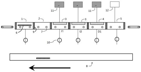
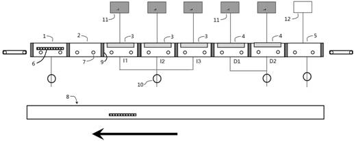
[0107] A coating device for heterojunction solar cells in this embodiment is used for depositing amorphous silicon-based thin films on heterojunction solar cells, which may include linearly arranged loading chamber 1, preheating chamber 2, process chamber, and unloading chamber The basic cavity structure required for processing such as cavity 5, among which:

[0108] Loading chamber 1: responsible for the entry of loading and loading carrier plates.

[0109] Preheating chamber 2: responsible for preheating the carrier board. Non-contact heating can be used to preheat the carrier plate to reach the temperature required by the process.

[0110] Process chamber: used for deposition and coating processing. According to the requirements of the process, feed the corresponding gas, use the vacuum pump 10 to form a vacuum environment or maintain the air pressure, use the plasma power supply and process gas 11 to form a processing environment, and perform intrinsic layer silicon thin...

Embodiment 2

[0119] This embodiment further limits the solution in Embodiment 1. The intrinsic process chamber and the doping process chamber are provided with a capacitively coupled flat plate structure for forming a thin film by chemical vapor deposition. The scheme preferably adopts plasma chemical vapor deposition to form a thin film. In this structure, a capacitively coupled flat plate structure is connected with an RF / VHF radio frequency power supply, and the frequency of the radio frequency power supply is 10MHz-100MHz.

[0120] When performing the silicon thin film coating of the intrinsic layer, the frequency of the radio frequency power supply between different intrinsic process chambers can be set as required.

[0121] The thickness and defect density of the intrinsic silicon thin film have an important impact on the conversion efficiency of the cell. By decomposing the intrinsic silicon thin film processing technology, it is easier to realize the control of process parameters fo...

Embodiment 3

[0124] In the heterojunction solar cell coating equipment of this embodiment, a roller mechanism is provided at the bottom of each cavity, and the carrier is transported by the roller mechanism.

[0125] combine figure 1 , the carrier does not move during the static coating process. When transmission is required, the speed of the carrier board can be moved at a speed of 90 ~ 800mm / s. When moving, the carrying pallet passes through the linearly arranged loading chamber 1, preheating chamber 2, I1 intrinsic process chamber, I2 intrinsic process chamber, D1 doping process chamber, and unloading chamber 5, and uses the roller mechanism to realize Transport of the carrier board.

[0126] More preferably, the speed of the carrier board can be controlled at 200-700 mm / s, and preferably, the conveying speed of the rollers is 300-600 mm / s. For example, a speed of 320 mm / s is used for motion.

[0127] If the speed is too high, the carrier plate is easy to vibrate, and the friction b...


PUM


Abstract

The invention discloses heterojunction solar cell coating equipment, method and system, a solar cell, an assembly and a power generation system, and belongs to the field of solar cell processing. Theheterojunction solar cell coating equipment is used for depositing a heterojunction solar cell amorphous silicon-based thin film, and comprises a process cavity, wherein the process cavity comprises at least two intrinsic process cavities used for deposition of an intrinsic layer silicon thin film process, and at least one doping process cavity used for deposition of an N-type silicon film or P-type silicon film process, and the cavities in the intrinsic process cavities and the doping process cavity are isolated by isolation valves. By combining the control of gas proportion and pressure, theequipment can process a plurality of solar cells at the same time, so that the overall processing efficiency is greatly improved, and the equipment is suitable for commercial use.

Description

technical field [0001] The invention relates to the technical field of solar cell processing, and more specifically, to a heterojunction solar cell coating device, method, system, solar cell, component, and power generation system. Background technique [0002] Silicon heterojunction solar cell is a cell technology that deposits amorphous silicon-based thin film on the surface of crystalline silicon to form a heterojunction. Compared with traditional crystalline silicon cells and silicon thin film cells, it has simple process, high power generation, and The advantage of low electricity cost has become a hot spot in the photovoltaic industry. [0003] Silicon heterojunction cells deposit intrinsic layer i / doped layer n or intrinsic layer i / doped layer p amorphous silicon-based thin films on the upper and lower surfaces of crystalline silicon by PECVD technology. This series of thin films are characterized by thin and multilayer , usually one type of amorphous silicon film re...

Claims


Application Information

Patent Timeline
IPC IPC(8): H01L31/0747H01L31/18C23C16/54C23C16/50C23C16/24
CPCH01L31/0747H01L31/1804C23C16/54C23C16/50C23C16/24Y02E10/547Y02P70/50H01L31/202
Inventor 周剑曹新民陈晨王登志王朝
Owner SUZHOU MAIZHENG TECH CO LTD
Why Eureka
Try Eureka