Surface photovoltage spectrum detection method for enhancing spatial resolution

A surface photovoltage and detection method technology, which is applied in the direction of measuring devices, analyzing materials, and material analysis through optical means, can solve the problem that the separation ability of photogenerated charges is limited, and ordinary conductive probes cannot meet the needs of weak signal measurement and photovoltage on the surface of nanoparticles. Small signal and other problems, to achieve the effect of enhancing the surface photovoltage signal, signal stability, and enhancing the intensity of the light field

Pending Publication Date: 2020-10-27
DALIAN INST OF CHEM PHYSICS CHINESE ACAD OF SCI
View PDF6 Cites 2 Cited by
  • Summary
  • Abstract
  • Description
  • Claims
  • Application Information

AI Technical Summary

Problems solved by technology

Moreover, due to the effective surface space charge layer width of these small particles, the separation ability of photogenerated charges is limited, so that the photovoltage signal generated by photoexcitation is very small, which brings challenges to the measurement of photovoltage signals on sample single particles.
Ordinary conductive probes cannot meet the measurement of weak signals on the surface of nanoparticles, and a test method that can enhance the surface photovoltage is urgently needed to obtain some information on the migration and separation of photogenerated charges on the surface of nanomaterials

Method used


Image

  • Surface photovoltage spectrum detection method for enhancing spatial resolution
  • Surface photovoltage spectrum detection method for enhancing spatial resolution
  • Surface photovoltage spectrum detection method for enhancing spatial resolution

Examples


Embodiment approach

[0034] 1 Fixing the p-Si single wafer on the conductive substrate;

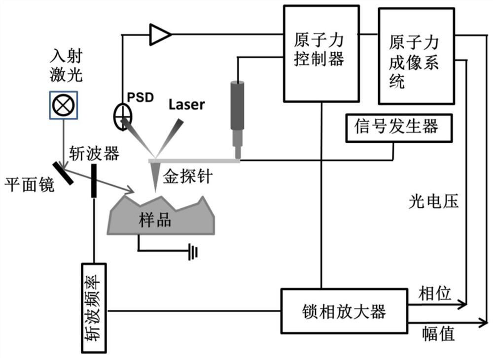
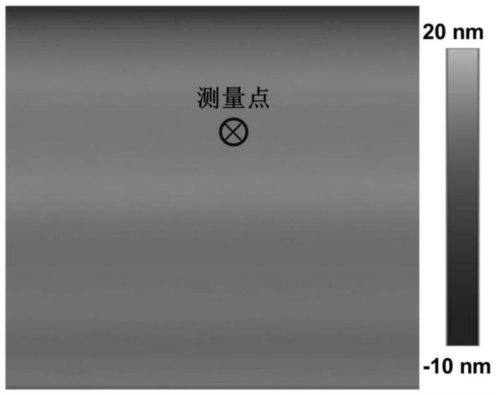
[0035] 2 Turn on the Kelvin force microscope, install the SCM-PIT probe, adjust the parameters, select the target position under the optical microscope, and scan the topography and potential value of the 2μm area on the sample surface, such as figure 2 ;

[0036] 3 Turn on the 638nm excitation light source, and focus the incident light onto the surface of the single crystal through a plane mirror;

[0037] 4 Convert the excitation light source into chopped light through a chopper;

[0038] 5 Turn on the lock-in amplifier, and input the potential output signal of the Kelvin force microscope and the frequency signal of the chopper into the lock-in amplifier;

[0039] 6 Connect the amplitude and phase signals of the photovoltage output by the lock-in amplifier to the Kelvin force microscope control system;

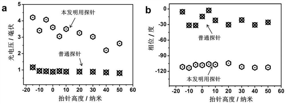
[0040] 7 Read the amplitude and phase values ​​of the photovoltage through software. choose figure...


PUM


Abstract

The invention discloses a surface photovoltage signal detection method for enhancing spatial resolution. The method comprises the following steps of: pretreating a sample, and starting a Kelvin forcemicroscope and a lock-in amplifier; installing a conductive probe plated with specific metals (gold, silver, copper and other metals with a plasma resonance effect); fixing the sample and adjusting scanning parameters; and starting a chopper, and recording photovoltage signals for enhancing spatial resolution of the sample. According to the testing method disclosed by the invention, the scanning probe plated with the specific metal has a local surface plasma resonance effect, so that the light field intensity of a sample region below the probe tip can be enhanced, and the surface photovoltagesignals can be remarkably enhanced. The enhanced surface photovoltage signals are stable and good in repeatability, and an idea is provided for detecting weak surface photovoltage signals.

Description

technical field [0001] The invention relates to a detection method and an application of a surface photovoltage spectrum with enhanced spatial resolution, belonging to the technical field of semiconductors. Background technique [0002] Photoelectric properties are important information to reflect the photoelectric conversion performance of materials. In order to effectively improve the photoelectric conversion efficiency, it is particularly important to understand the generation, transfer and separation process of photogenerated charges in photoelectric materials. Surface photovoltage spectroscopy is a technology and method mainly used to analyze the transition and transfer process of photogenerated charges on the surface and interface of semiconductor materials. This technique has the advantages of no need for sample labeling, fast response, high sensitivity, and no sample damage. It is an important means to determine the photoelectric response, conductivity type, energy b...

Claims


Application Information

Patent Timeline
Patent Type & Authority Applications(China)
IPC IPC(8): G01N21/552G01Q60/30G01Q60/46
CPCG01N21/554G01Q60/30G01Q60/46
Inventor 李灿高玉英范峰滔
Owner DALIAN INST OF CHEM PHYSICS CHINESE ACAD OF SCI
Why Eureka
Try Eureka