Plasma-induced transparent metamaterial sensor

A technology for inducing transparency and plasma, which can be used in semiconductor devices, material excitation analysis, thermal excitation analysis, etc., and can solve the problem of fixed operating wavelength of transparent windows.

Pending Publication Date: 2020-10-27
CHINA JILIANG UNIV
View PDF0 Cites 6 Cited by
  • Summary
  • Abstract
  • Description
  • Claims
  • Application Information

AI Technical Summary

Problems solved by technology

It is well known that the plasmonic transparency effect based on the excitation of conventional metallic metamaterials has a serious disadvantage that the operating wavelength of the transparent window is fixed once the structure is fabricated.

Method used


Image

  • Plasma-induced transparent metamaterial sensor
  • Plasma-induced transparent metamaterial sensor
  • Plasma-induced transparent metamaterial sensor

Examples


Embodiment Construction

[0020] The following is a specific embodiment of the present invention and in conjunction with the accompanying drawings, further describes the technical solution of the present invention, but the present invention is not limited to this embodiment.

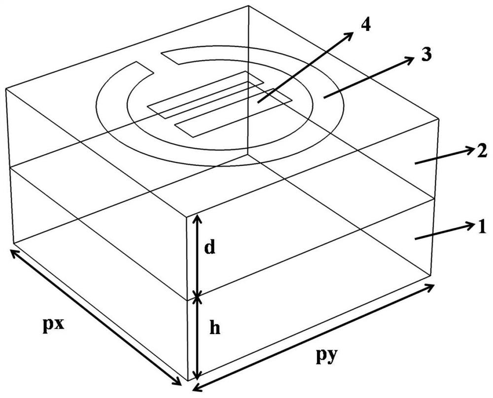
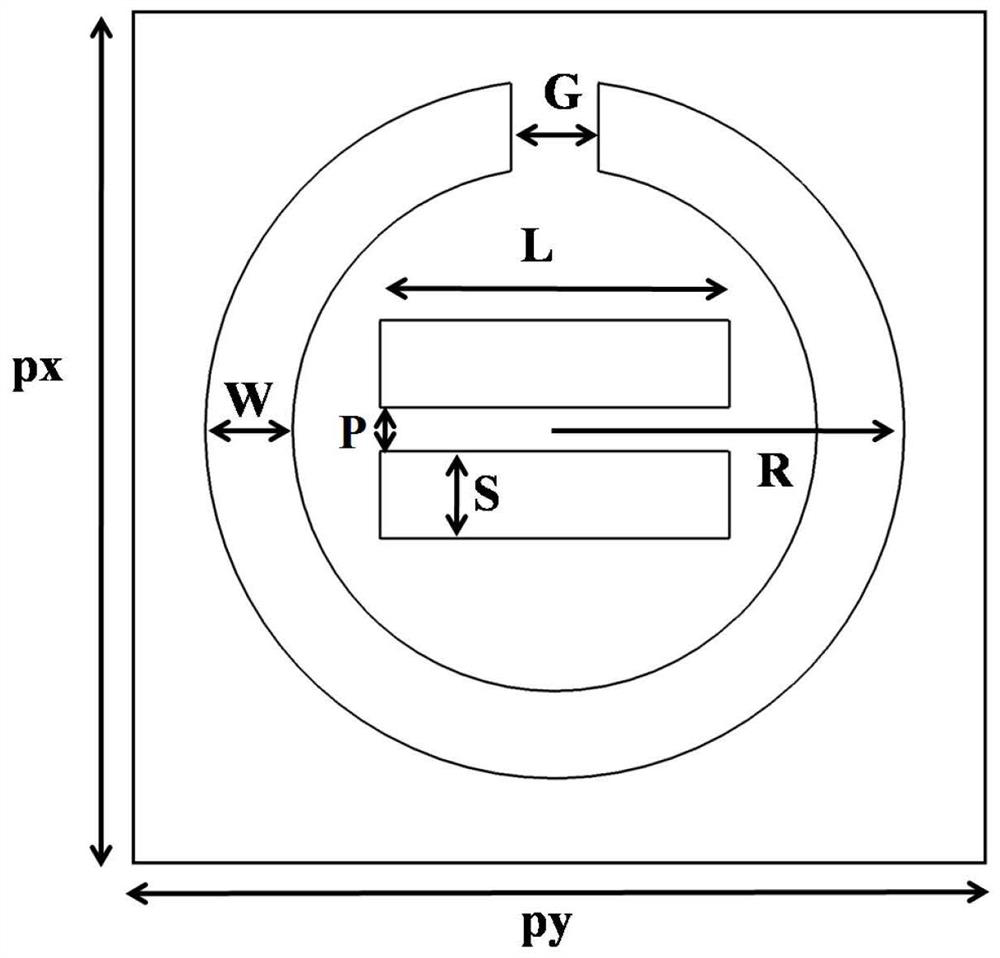
[0021] attached figure 1 A schematic diagram of a unit structure of a plasmon-induced transparent metamaterial sensor. The length and width of the structural unit are px and py, the thickness of the doped silicon base layer is h, the thickness of the silicon dioxide dielectric layer is d, the thickness of the graphene split resonator ring and the graphene double nanoribbon is 1nm, and the graphene opening The radius length of the resonant ring is R, the gap width of the split resonant ring is G, the width of the split resonant ring is W, the length of the double nanoribbon is L, the width of the double nanoribbon is S, and the spacing between the double nanoribbons is P, Graphene split resonator ring-double nanoribbon structure ...


PUM

PropertyMeasurementUnit
Thicknessaaaaaaaaaa
Gap widthaaaaaaaaaa
Widthaaaaaaaaaa

Abstract

The invention discloses a plasma-induced transparent metamaterial sensor, which belongs to a sensing device of a graphene material in an intermediate infrared band, and utilizes graphene surface plasma characteristics and a plasma-induced transparency theory. The sensing device is of a three-dimensional periodic structure and is of a three-layer structure composed of a top layer, a middle layer and a bottom layer which are stacked from top to bottom, wherein the top layer is of a graphene split-ring resonator and graphene double-nanobelt structure, the middle layer is a silicon dioxide medium,and the bottom layer is a doped silicon substrate layer. The resonance spectrum of the plasma-induced transparent metamaterial sensor is calculated and simulated mainly through a finite element method, the structure of the sensor is optimized, the capability of exciting plasma-induced transparent resonance in a middle-infrared frequency band is achieved, and the linearity and resonance frequencyof the plasma-induced transparent resonance can be effectively tuned. The sensor is simple, compact and reasonable in structure and convenient to machine.

Description

technical field [0001] The invention relates to a plasma-induced transparent metamaterial sensor, which belongs to the application field of graphene materials in mid-infrared band sensor devices. Background technique [0002] Electromagnetically induced transparency (EIT) is a phenomenon of absorption-transmission enhancement caused by quantum interference, which enables the control of the optical response of materials with electromagnetic fields. This phenomenon was first observed in atomic systems, and it can be realized in three-level systems. The atomic EIT effect has been widely used in slow light, nonlinear optics and other fields. However, the realization of the atomic EIT effect is very difficult and requires very harsh environmental and operating conditions, which greatly limits the application and development of traditional atomic EIT. In order to overcome these problems, a new system similar to the atomic EIT system has been studied. Plasmon-induced transparenc...

Claims


Application Information

Patent Timeline
IPC IPC(8): G01N21/71H01L31/028H01L31/101H01L31/0352
CPCG01N21/71H01L31/028H01L31/0352H01L31/101
Inventor 肖丙刚宫绍康蔡万钧
Owner CHINA JILIANG UNIV
Why Eureka
Try Eureka