Rare earth electroluminescent blue light device

A rare earth and device technology, applied in the field of rare earth electro-optical blue light devices, can solve the problems of easy aging, poor stability of organic matter, blue light color distortion, etc.

Active Publication Date: 2020-10-27
HUAZHONG UNIV OF SCI & TECH
View PDF3 Cites 3 Cited by
  • Summary
  • Abstract
  • Description
  • Claims
  • Application Information

AI Technical Summary

Problems solved by technology

[0004] Aiming at the above defects or improvement needs of the prior art, the present invention provides a rare-earth electroluminescent blue light device to solve the technical problems of the prior art that organic matter is used as a luminescent material, and the organic matter is poor in stability, easy to age and easily leads to color distortion of blue light

Method used


Image

  • Rare earth electroluminescent blue light device
  • Rare earth electroluminescent blue light device
  • Rare earth electroluminescent blue light device

Examples


Embodiment 1

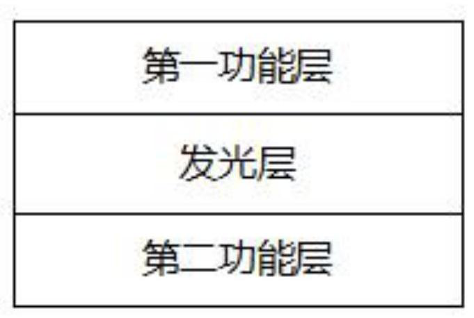
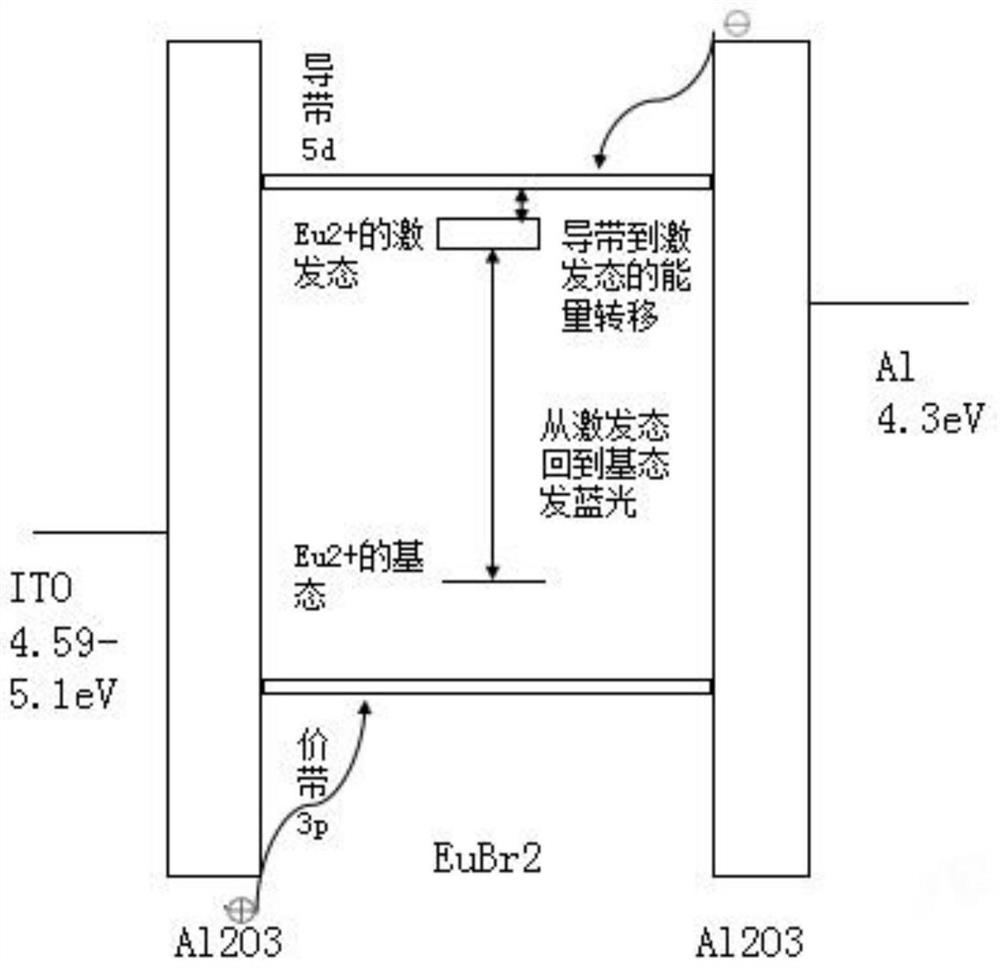
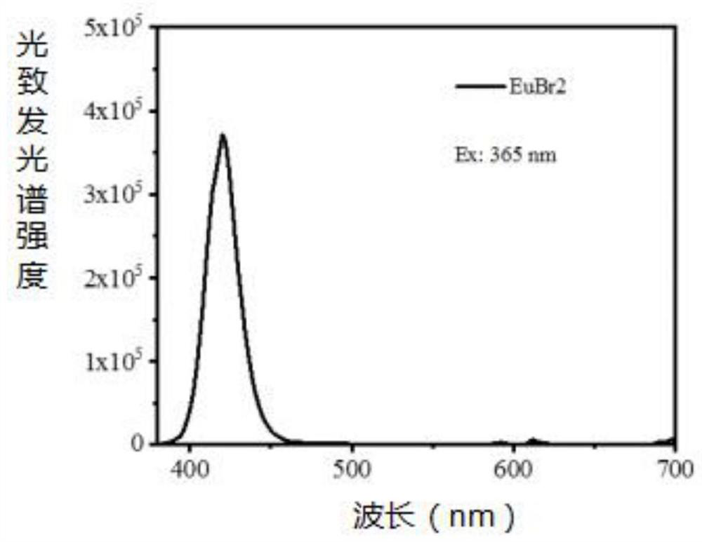
[0040] In this embodiment, the light-emitting layer material is EuBr 2 , functional layer material is Al 2 o 3 Taking the electroluminescent blue light device of high dielectric constant material as an example, its specific preparation method includes the following steps:

[0041] a) Use detergent, deionized water, acetone and absolute ethanol to ultrasonically clean the substrate ITO in sequence, for half an hour each time; where, ITO uses a substrate that has been etched two times, and its light-emitting area is about 2mm*2mm;

[0042] b) Depositing Al on ITO by atomic layer deposition (Atomic layer deposition, ALD) process 2 o 3 thin film, about 3nm thick;

[0043] c) will be plated Al 2 o 3 The substrate of the film is placed in the evaporation glove box, and the vacuum degree is evacuated to 4*10 -5 Below Pa, evaporate EuBr at a speed of 0.1nm / s 2 Thin films were evaporated to a thickness of 100nm in total. After the evaporation is completed, take the substrate i...

Embodiment 2

[0047] In this embodiment, the light-emitting layer material is CsEuBr 3 , functional layer material is Al 2 o 3 Taking the electroluminescent blue light device of high dielectric constant material as an example, its specific preparation method includes the following steps:

[0048] a) Ultrasonic cleaning the ITO substrate with detergent, deionized water, acetone and absolute ethanol in sequence, half an hour each time; among them, ITO uses a substrate that has been etched two times, and its light-emitting area is about 2mm*2mm;

[0049] b) Depositing Al on ITO by ALD process 2 o 3 thin film, about 3nm thick;

[0050] c) will be plated Al 2 o 3 The substrate of the film is placed in the evaporation glove box, and the vacuum degree is evacuated to 4*10 -5 Below Pa, use the double-source co-evaporation method to evaporate EuBr at a speed of 0.1nm / s 2 Thin film, evaporate a CsBr thin film at a speed of 0.1nm / s, with a total thickness of 100nm; after the evaporation is com...

Embodiment 3

[0054] In this embodiment, the light-emitting layer material is Cs 2 EuBr 4 , functional layer material is Al 2 o 3 Taking the electroluminescent blue light device of high dielectric constant material as an example, its specific preparation method includes the following steps:

[0055] a) Use detergent, deionized water, acetone and absolute ethanol to ultrasonically clean the substrate ITO in sequence, for half an hour each time; where, ITO uses a substrate that has been etched two times, and its light-emitting area is about 2mm*2mm;

[0056] b) Depositing Al on ITO by ALD process 2 o 3 thin film, about 3nm thick;

[0057] c) will be plated Al 2 o 3 The substrate of the film is placed in the evaporation glove box, and the vacuum degree is evacuated to 4*10 -5 Below Pa, use the double-source co-evaporation method to evaporate EuBr at a speed of 0.1nm / s 2 For the thin film, a CsBr thin film was evaporated at a speed of 0.2nm / s, and a total thickness of 100nm was evapora...


PUM

PropertyMeasurementUnit
wavelengthaaaaaaaaaa

Abstract

The invention discloses a rare earth electroluminescent blue light device. The rare earth electroluminescent blue light device comprises a first functional layer, a light emitting layer and a second functional layer which are sequentially arranged from top to bottom, wherein the material of the light emitting layer is rare earth halide or a derivative thereof, the light emitting layer is of a non-doped type, and the transition mode of rare earth ions is f-d allowed transition. As the material is an inorganic material, the material is good in stability, not easy to age and long in service life,and has the property that the light-emitting peak position is adjustable by a crystal field, the crystal field of the material can be adjusted by changing the crystallinity of the material in the process of preparing the light emitting layer, and then the light-emitting peak position of rare earth ions in the material is adjusted so as to generate pure blue light. Furthermore, the material of thelight emitting layer has the light-emitting property of f-d allowed transition, so that the emission intensity is high, and the brightness is high. Due to the fact that the f-d non-doped rare earth compound 5d track contributes to the conduction band or valence band of the compound, large charge injection can be achieved, and blue light generated by the organic electroluminescent blue light device is enabled to have high external quantum efficiency and high brightness.

Description

technical field [0001] The invention belongs to the field of optoelectronic devices, and more specifically relates to a rare-earth electro-induced blue light device. Background technique [0002] Electro-blue light device (blue LED) is the core technology in the display field, which has a huge application market and high national strategic significance. With the advancement of science and technology and the development of society, electro-blue light technology also needs new breakthroughs. To meet the urgent needs of high stability, high brightness, etc., it is of great significance to study an electroluminescent blue light device. [0003] Existing electroluminescent blue light devices mainly include: blue light organic light-emitting diode (Organic Light-Emitting Diode, OLED), blue light quantum dot light-emitting diode (Quantum dot Light-Emitting Diode, QLED) and blue light perovskite light-emitting diode (Perovskite Light-Emitting Diode). Diode, PeLED); Among them, OLED...

Claims


Application Information

Patent Timeline
Patent Type & Authority Applications(China)
IPC IPC(8): H01L33/26H01L51/50H01L33/00H01L51/00
CPCH01L33/26H01L33/005H10K71/12H10K71/15H10K50/115
Inventor 唐江杨龙波谭智方高亮胡浩
Owner HUAZHONG UNIV OF SCI & TECH
Why Eureka
Try Eureka