Stress regulation and control unit structure and method for spin wave transmission characteristics
A technology of transmission characteristics and stress regulation, applied in the parts of electromagnetic equipment, the manufacture/processing of electromagnetic devices, etc., can solve the problems of high energy consumption and complex structure, achieve low efficiency, solve high energy consumption, solve heat loss and static The effect of power consumption
- Summary
- Abstract
- Description
- Claims
- Application Information
AI Technical Summary
Problems solved by technology
Method used
Image
Examples
Embodiment 1
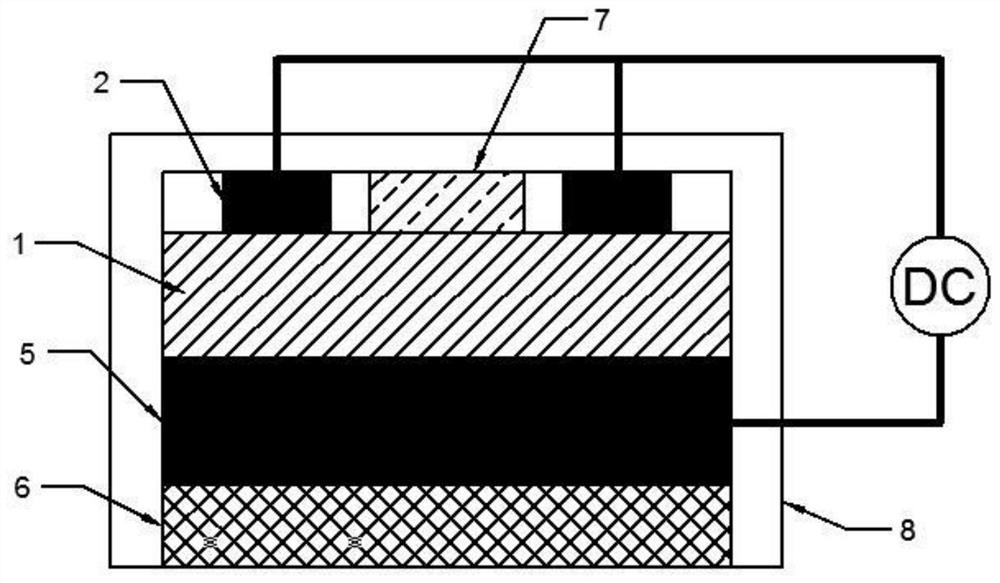
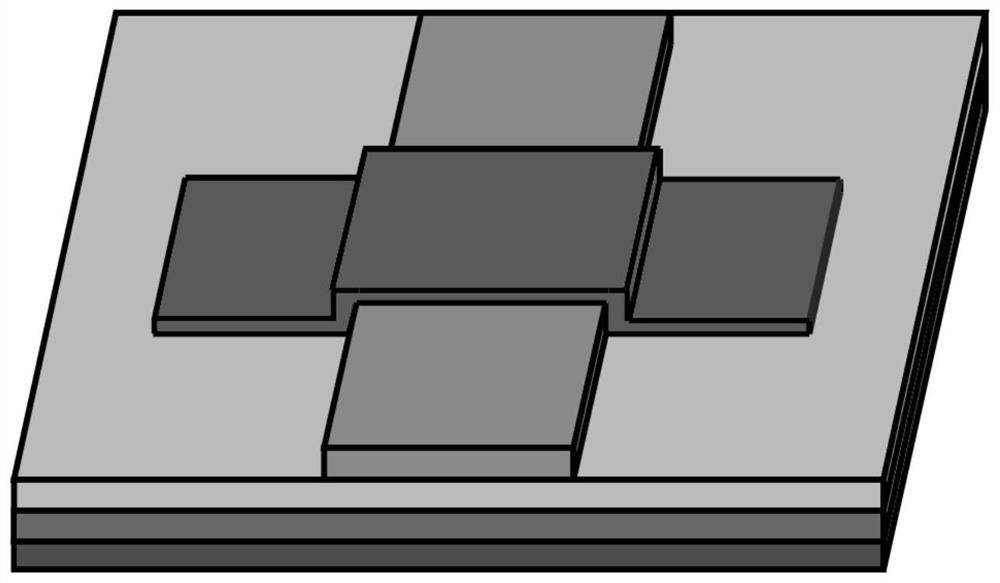
[0028] This embodiment proposes a stress control unit structure and method for spin wave transmission characteristics, and controls spin wave phase, amplitude and other related features so as to be applied to spin electronic devices to realize various logic functions. Such as figure 1 As shown, the control unit is composed of a substrate layer 6 , a spin wave guide layer 7 , a bottom electrode layer 5 , a control layer 1 , a top electrode 2 and a protective layer 8 . The attached drawings are schematic diagrams, and the sizes and thicknesses of the functional layers involved are not actual sizes, and there are many choices of materials, depending on actual needs.
[0029] The regulating unit structure proposed by the present invention can be applied to various spin wave waveguide structures, depending on specific applications, and the size of the unit structure is not limited. Most of the waveguide materials are ferromagnetic materials with magnetostrictive effect, which can ...
Embodiment 2
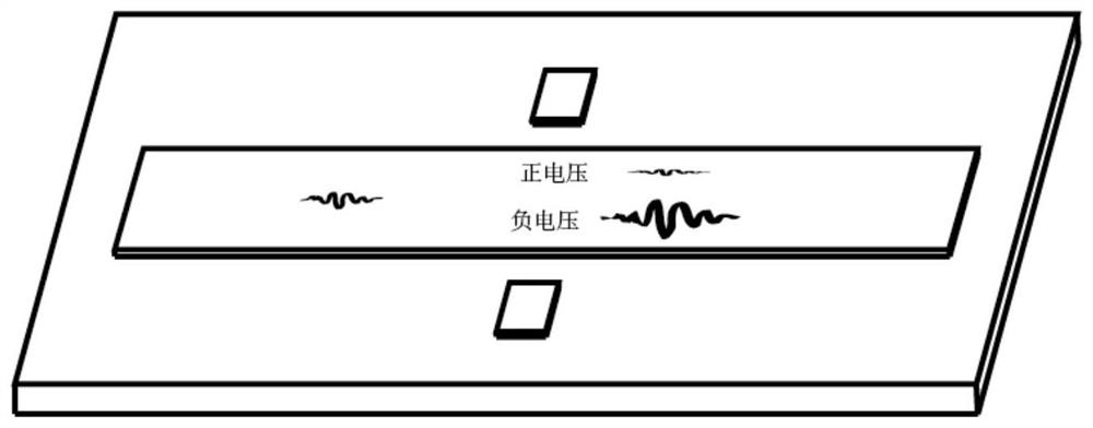
[0035]In this embodiment, a device unit structure based on spin wave propagating in cobalt-iron-boron (CoFeB) is taken as an example to specifically illustrate the structure, function and application of the present invention. Refer to attached image 3 , give a typical structural embodiment of the present invention: a strip-shaped spin-wave waveguide.
[0036] In this example, the main structure for adjusting the spin wave transmission characteristics uses cobalt-iron-boron (CoFeB) material with a length of 2000 nm, a width of 100 nm, and a thickness of 0.8 nm. The propagation mode of the spin wave is forward bulk wave, that is, the mode in which the spin wave propagation direction is perpendicular to the direction of the magnetic field. The bottom is the control layer, the top is the spin wave waveguide layer, and the top double electrode is made of conductive material copper (Cu), which is located on both sides of the magnetic material and is symmetrical. The control layer...
Embodiment 3
[0049] Refer to attached Figure 7 , provide four typical logic application embodiments of the present invention: single-channel logic structure, single-channel series logic structure, dual-channel parallel logic structure, and dual-channel series-parallel logic structure. What needs to be explained here is: 1. This implementation The example is not limited to the above logical structure, there can be more branches and control unit combination, 2, a single control unit can adjust the spin wave amplitude, phase and other functions through voltage, in the logic structure proposed in this embodiment It is not limited to using one of the functions, but may be any one of the functions or any combination of multiple functions. In order to realize more complex logical calculation functions.
[0050] The logic device is based on the structure proposed by the present invention, that is, a stress regulation unit structure with spin wave transmission characteristics and a spin wave tran...
PUM
| Property | Measurement | Unit |
|---|---|---|
| Length | aaaaa | aaaaa |
| Width | aaaaa | aaaaa |
| Thickness | aaaaa | aaaaa |
Abstract
Description
Claims
Application Information


