
Wafer level backside adhesive tape, and manufacturing method therefor

A wafer-level, back-side technology, applied in semiconductor/solid-state device manufacturing, adhesives, adhesive types, etc., can solve problems such as cracks, improper sawing lines, and product detachment

Inactive Publication Date: 2020-11-06
ONOHAKOBI TECH INST CO LTD
View PDF11 Cites 0 Cited by
  • Summary
  • Abstract
  • Description
  • Claims
  • Application Information

AI Technical Summary

Problems solved by technology

[0012] Also, the existing sheet for forming a protective film is made by making a layer of a thermosetting resin mixed with a black pigment and a binder polymer, a thermosetting agent, or an ultraviolet curing agent, and therefore, when the thermosetting resin is not When fully cured, there may be a problem of product detachment due to reduced adhesion when transported to the next process after being attached to the backside of the wafer (lamination process)
[0013] Also, for the thermosetting resin, laser marking can be performed in a cured state, but cracks or chipping may occur during the cutting process depending on the curing state of the resin (Chipping: Dicing process). When sawing (Saw Line) is not correct and the shape is torn), etc.
And, in the reflow soldering (Reflow) process in the subsequent process, the corners of the cured resin are broken and spread into cracks (Crack), therefore, the entire surface of the wafer may be contaminated by the cured resin powder
[0014] In this case, the wafer requires 2 to 3 separate washing processes, and there is also the problem of additional cost to maintain / maintain the reflow soldering machine due to contamination of the reflow soldering machine by the cured resin powder

Method used


Image

  • Wafer level backside adhesive tape, and manufacturing method therefor
  • Wafer level backside adhesive tape, and manufacturing method therefor
  • Wafer level backside adhesive tape, and manufacturing method therefor

Examples


Embodiment 1

[0083] A PET film obtained by corona-treating one side surface of a PET film with a thickness of about 12 μm that was primer-coated with a thermosetting acrylic coating agent was prepared.

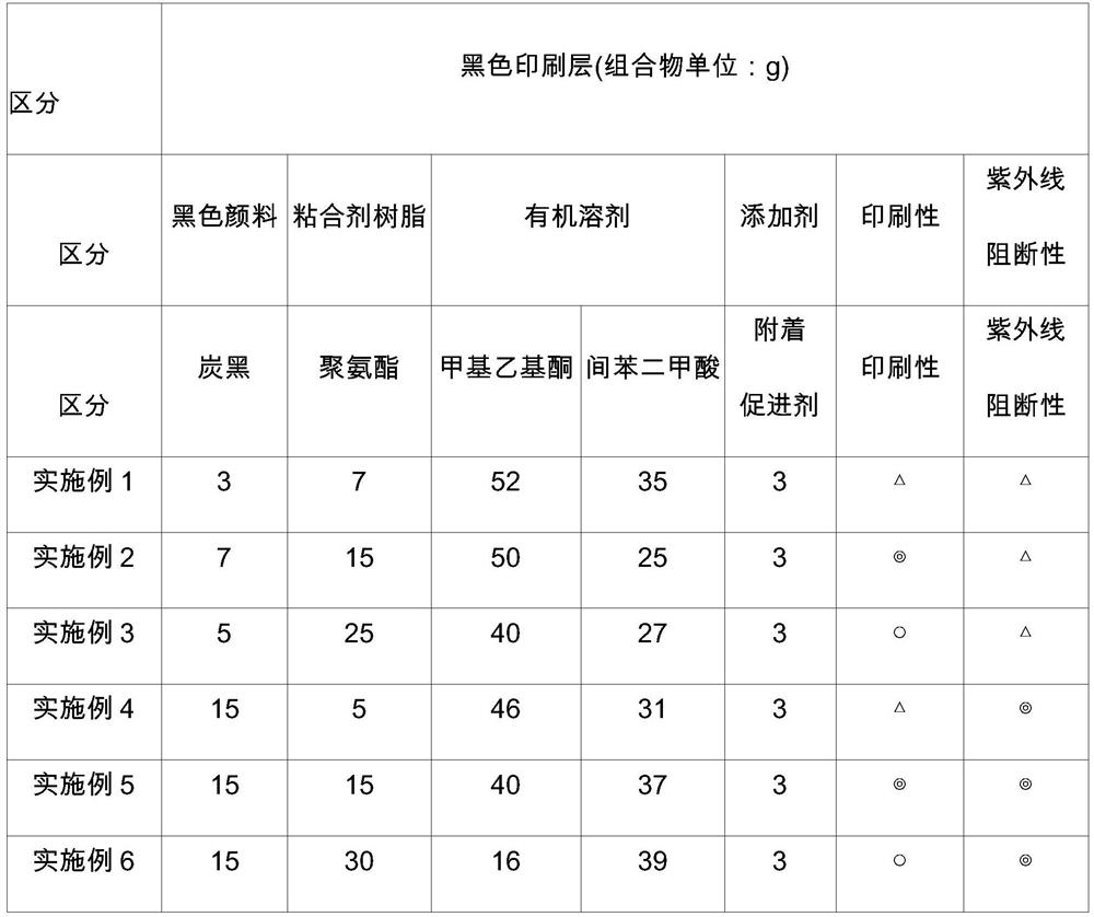
[0084] Thereafter, a black printing layer coating liquid of 5 g of carbon black, 15 g of polyurethane resin, 77 g of an organic solvent consisting of 52 g of methyl ethyl ketone and 25 g of isopropyl alcohol, and 3 g of adhesion promoter BYK-4500 was mixed using the gravure printing method A PET film having a black printed layer having a thickness of about 3.5 μm was formed by coating on one side surface of the corona-treated PET film.

Embodiment 2

[0086] A PET film obtained by corona-treating one side surface of a PET film with a thickness of about 12 μm that was primer-coated with a thermosetting acrylic coating agent was prepared.

[0087] Thereafter, a black printing layer coating solution that mixed 7 g of carbon black, 15 g of polyurethane resin, 75 g of an organic solvent consisting of 50 g of methyl ethyl ketone and 25 g of isopropyl alcohol, and 3 g of adhesion promoter BYK-4500 was mixed using the gravure printing method A PET film having a black printing layer having a thickness of about 3.5 μm was formed by coating on one side surface of the corona-treated PET film.

Embodiment 3

[0089] A PET film obtained by corona-treating one side surface of a PET film with a thickness of about 12 μm that was primer-coated with a thermosetting acrylic coating agent was prepared.

[0090] Thereafter, a black printing layer coating liquid that mixed 5 g of carbon black, 25 g of polyurethane resin, 67 g of an organic solvent consisting of 40 g of methyl ethyl ketone and 27 g of isopropyl alcohol, and 3 g of adhesion promoter BYK-4500 was mixed using the gravure printing method A PET film having a black printing layer having a thickness of about 3.5 μm was formed by coating on one side surface of the corona-treated PET film.


PUM

PropertyMeasurementUnit
thicknessaaaaaaaaaa
particle sizeaaaaaaaaaa
thicknessaaaaaaaaaa

Abstract

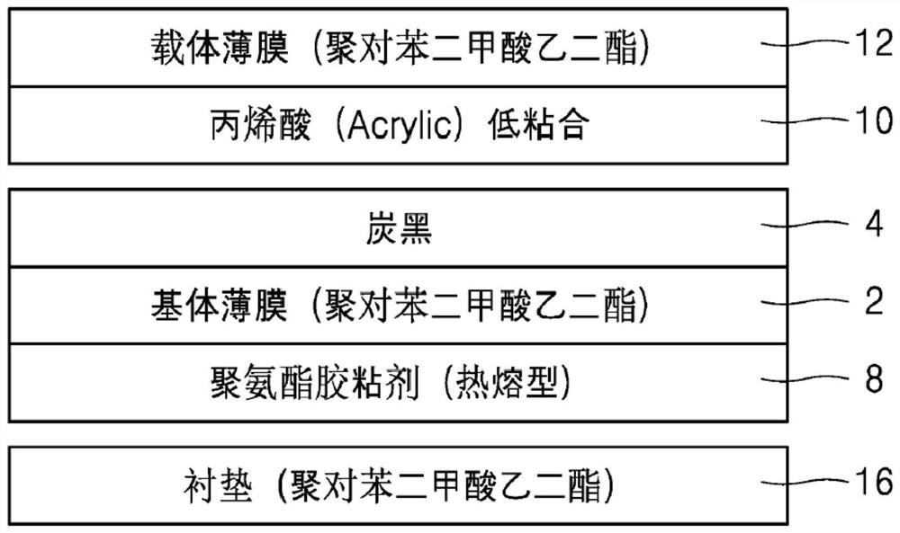
The present invention comprises a wafer level backside adhesive tape comprising: a sheet-shaped substrate; a black printed layer layered on one surface of the substrate, blocking ultraviolet rays, andfacilitating the visibility of laser marking; a hot-melt adhesive layer layered on the other surface of the substrate, opposite to the one surface on which the black printed layer is layered; and anacrylic low-adhesive carrier layer layered on the black printed layer and comprising an acryl enabling thermal adhesion.

Description

technical field [0001] The present invention relates to a wafer-level back tape and a manufacturing method thereof, and more particularly, relates to a wafer-level adhesive tape capable of performing laser marking (Laser Marking) and enduring a cutting (Dicing) process while protecting exposed chips. wafer-level backside tape on the backside of the Background technique [0002] As a method of attaching (mounting) a semiconductor chip to a circuit substrate, there is a method of direct welding using an electrode pattern on the lower surface of the chip without using an intermediate medium such as a metal wire or a ball grid array (BGA; Ball grid array), which This method is called the flip chip method. [0003] The flip-chip method has the following advantages: Since the size of the package is the same as the chip size as a leadless semiconductor without wires, miniaturization and weight reduction can be achieved, and the pitch between electrodes can be finely adjusted. ). ...

Claims


Application Information

Patent Timeline
Patent Type & Authority Applications(China)
IPC IPC(8): C09J7/29H01L21/67H01L21/683C09J133/00
CPCC08K3/04C09J133/08C09J2203/326C09J2475/00C09J7/29C09J2301/304C09J2301/312C09J2301/41H01L23/29H01L23/3164H01L23/544H01L2223/54486C09J133/00H01L21/67132H01L21/6836
Inventor 全成浩罗丙淳
Owner ONOHAKOBI TECH INST CO LTD
Learn More