
Cellular structure of silicon carbide device, preparation method of cellular structure and silicon carbide device

A silicon carbide and silicon carbide substrate technology, applied in semiconductor/solid-state device manufacturing, semiconductor devices, electrical components, etc., can solve problems such as deterioration, device failure reliability, etc.

Active Publication Date: 2020-11-13
ZHUZHOU CRRC TIMES SEMICON CO LTD
View PDF5 Cites 7 Cited by
  • Summary
  • Abstract
  • Description
  • Claims
  • Application Information

AI Technical Summary

Problems solved by technology

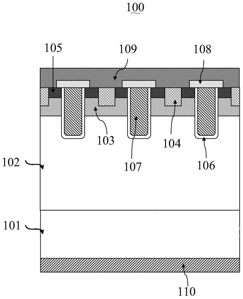
[0004] In view of the above problems, the present disclosure provides a cell structure of a silicon carbide device, its preparation method and a silicon carbide device, which solves the problem that the silicon carbide device in the prior art is in the blocking state due to the concentrated electric field that damages the gate oxide layer. Technical problems of failure and poor reliability

Method used


Image

  • Cellular structure of silicon carbide device, preparation method of cellular structure and silicon carbide device
  • Cellular structure of silicon carbide device, preparation method of cellular structure and silicon carbide device
  • Cellular structure of silicon carbide device, preparation method of cellular structure and silicon carbide device

Examples


Embodiment 1

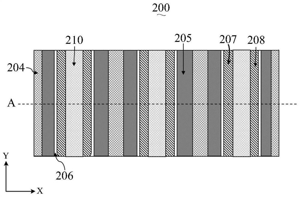
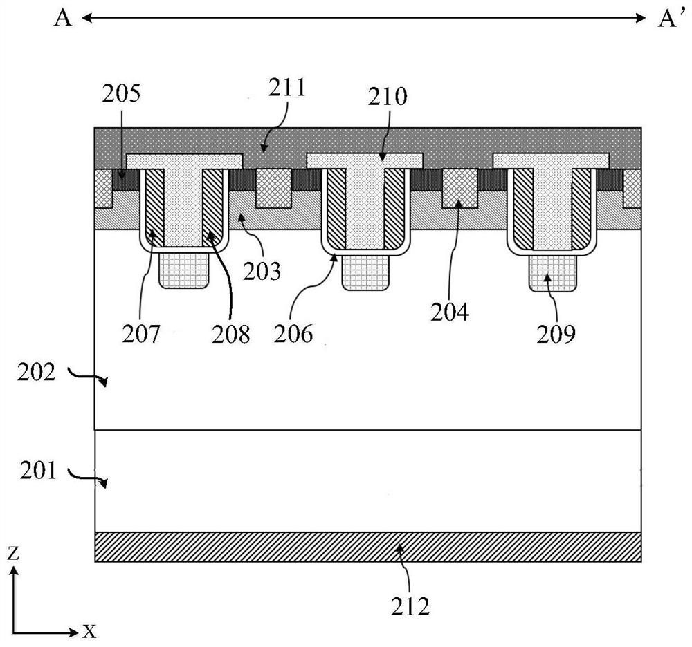
[0102] Such as figure 2 and image 3As shown, the embodiment of the present disclosure provides a cell structure 200 of a silicon carbide device, including a substrate 201, a drift layer 202, a well region 203, a first source region 204, a second source region 205, a first gate trench (not marked in the figure), gate oxide layer 206 , first gate 207 , second gate 208 , first shielding region 209 , interlayer dielectric layer 210 , source metal layer 211 and drain metal layer 212 .

[0103] It should be noted that, in order to figure 2 Clearly show the first source region 204, the second source region 205, the first gate trench (not marked in the figure), the gate oxide layer 206, the first gate 207, the second gate 208 and the interlayer dielectric layer 210 shape and position, so figure 2 The substrate 201, the drift layer 202, the well region 203, the first shielding region 209, the source metal layer 211 and the drain metal layer 212, as well as the first gate 207 and...

Embodiment 2

[0120] Such as Figure 4 and Figure 5 As shown, the embodiment of the present disclosure provides another cell structure 300 of a silicon carbide device, including a substrate 301, a drift layer 302, a well region 303, a first source region 304, a second source region 305, a first gate trench Groove (not marked in the figure), second gate trench (not marked in the figure), first shielding area 306, second shielding area 307, gate oxide layer 308, first gate 309, second gate 310 , a third gate 311 , a fourth gate 312 , an interlayer dielectric layer 313 , a source metal layer 314 and a drain metal layer 315 .

[0121] It should be noted that, in order to Figure 4 Clearly show the first source region 304, the second source region 305, the first gate trench (not marked in the figure), the second gate trench (not marked in the figure), the gate oxide layer 308, the first gate 309, the shapes and positions of the second gate 310, the third gate 311, the fourth gate 312 and the...

Embodiment 3

[0140] On the basis of the first embodiment, this embodiment provides a method for preparing a cell structure 200 of a silicon carbide device. Figure 6 It is a schematic flowchart of a method for preparing a cell structure 200 of a silicon carbide device shown in an embodiment of the present disclosure. Figure 7-Figure 13 It is a schematic cross-sectional structure formed by related steps of a method for manufacturing a silicon carbide device cell structure 200 shown in an embodiment of the present disclosure. Below, refer to Figure 6 and Figure 7-Figure 13 The detailed steps of an exemplary method of the method for manufacturing the cell structure 200 of the silicon carbide device proposed by the embodiment of the present disclosure will be described.

[0141] Such as Figure 6 As shown, the method for preparing the cellular structure 200 of the silicon carbide device in this embodiment includes the following steps:

[0142] Step S201: if Figure 7 As shown, a silico...


PUM

PropertyMeasurementUnit
depthaaaaaaaaaa
thicknessaaaaaaaaaa
thicknessaaaaaaaaaa

Abstract

The invention provides a cellular structure of a silicon carbide device, a preparation method of the cellular structure and the silicon carbide device. The cellular structure comprises a plurality ofsecond conductive type well regions arranged in the surface of a drift layer at intervals, a second conductive type first source region and a first conductive type second source region which are located in the surface of the well region, first gate trenches located between every two adjacent well regions, a second conductive type first shielding region which is located in the drift layer and located below the first gate trenches, and a first gate and a second gate which are arranged in the first gate trench and are respectively located on two sides of the first gate trench. By arranging the first shielding region at the bottom of the first gate trench, the electric field stress of a gate oxide layer of the device in a blocking state can be greatly reduced, and the long-term use reliabilityof the device is greatly improved. The first gate and the second gate which are isolated by the interlayer dielectric layer are arranged in the gate trench to form a split gate, so that the parasiticcapacitance of the gate can be reduced.

Description

technical field [0001] The present disclosure relates to the technical field of semiconductor devices, in particular to a cell structure of a silicon carbide device, a preparation method thereof, and a silicon carbide device. Background technique [0002] Silicon carbide (SiC) is a new wide-bandgap semiconductor material with excellent physical, chemical and electrical properties. The breakdown electric field strength of silicon carbide is 10 times that of traditional silicon, the thermal conductivity is 3 times that of silicon, and it has a higher switching frequency, which can reduce the loss and volume of energy storage components in the circuit. In theory, silicon carbide devices can work in a high temperature environment above 600 °C, and have excellent radiation resistance, which greatly improves their high temperature stability. This makes SiC-based power semiconductor devices very attractive and promising for high-power and high-temperature applications. Among them...

Claims


Application Information

Patent Timeline
Patent Type & Authority Applications(China)
IPC IPC(8): H01L29/78H01L29/423H01L29/06H01L21/04
CPCH01L29/7813H01L29/4236H01L29/0696H01L21/049H01L29/66068Y02B70/10H01L29/1608H01L29/0623H01L29/4238
Inventor 王亚飞刘启军马亚超陈喜明刘坤李诚瞻罗海辉
Owner ZHUZHOU CRRC TIMES SEMICON CO LTD
Learn More