
Cellular structure of silicon carbide device, preparation method thereof and silicon carbide device

A silicon carbide and device technology, which is applied in semiconductor/solid-state device manufacturing, semiconductor devices, electrical components, etc., can solve problems such as variation, device failure reliability, etc., and achieve low manufacturing cost, which is conducive to current sharing and manufacturability strong effect

Pending Publication Date: 2021-04-06
ZHUZHOU CRRC TIMES SEMICON CO LTD
View PDF9 Cites 8 Cited by
  • Summary
  • Abstract
  • Description
  • Claims
  • Application Information

AI Technical Summary

Problems solved by technology

[0004] In view of the above problems, the present disclosure provides a cell structure of a silicon carbide device, its preparation method and a silicon carbide device, which solves the problem that the silicon carbide device in the prior art is damaged by the electric field stress to the gate dielectric layer in the blocking state and causes the device to Technical problems of failure and poor reliability

Method used


Image

  • Cellular structure of silicon carbide device, preparation method thereof and silicon carbide device
  • Cellular structure of silicon carbide device, preparation method thereof and silicon carbide device
  • Cellular structure of silicon carbide device, preparation method thereof and silicon carbide device

Examples


Embodiment 1

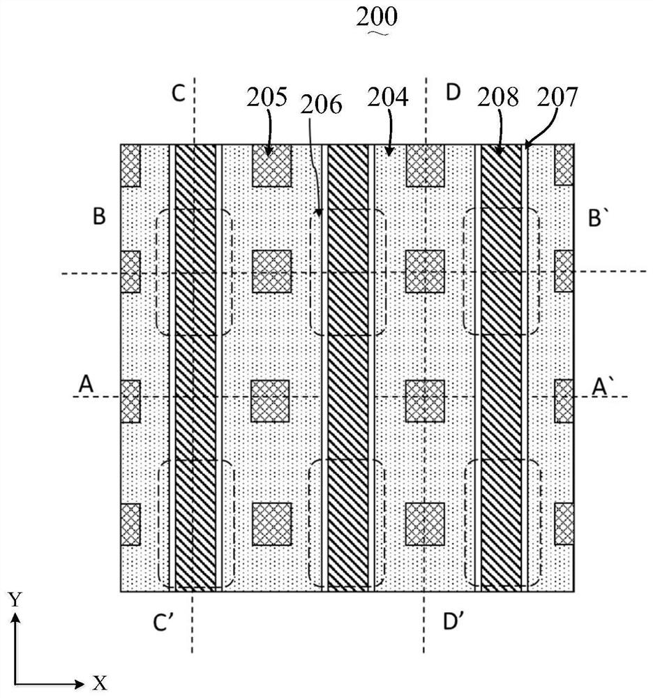
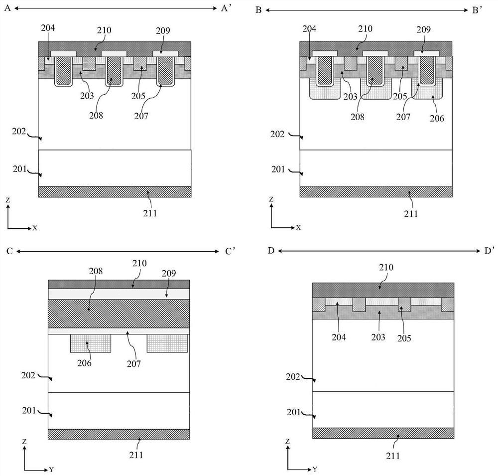
[0083] Such as figure 2 and image 3 As shown, the embodiment of the present disclosure provides a cell structure 200 of a silicon carbide device, including a substrate 201, a drift layer 202, a well region 203, a source region (not marked in the figure), a shield region 206, and a gate trench ( Not marked in the figure), gate dielectric layer 207 , gate 208 , interlayer dielectric layer 209 , source metal layer 210 and drain metal layer 211 .

[0084] It should be noted that, in this embodiment, the following "horizontal" refers to "X direction", "longitudinal" refers to "Y direction", "width" refers to "width in X direction", and depth refers to "Z direction". depth".

[0085] It should be noted that, in order to figure 2 The shapes and positions of the source region (not marked in the figure), the shielding region 206, the gate trench (not marked in the figure), the gate dielectric layer 207 and the gate 208 are clearly shown in the figure, so figure 2 The substrate ...

Embodiment 2

[0108] Such as Figure 4 and Figure 5 As shown, the embodiment of the present disclosure provides a cell structure 300 of a silicon carbide device, including a substrate 301, a drift layer 302, a well region 303, a source region (not marked in the figure), a shielding region 306, and a gate trench ( Not marked in the figure), gate dielectric layer 307 , gate 308 , interlayer dielectric layer 309 , source metal layer 310 and drain metal layer 311 .

[0109] It should be noted that, in this embodiment, the following "horizontal" refers to "X direction", "longitudinal" refers to "Y direction", "width" refers to "width in X direction", and depth refers to "Z direction". depth".

[0110] It should be noted that, in order to Figure 4 The shapes and positions of the source region (not marked in the figure), the shielding region 306, the gate trench (not marked in the figure), the gate dielectric layer 307 and the gate 308 are clearly shown in the figure, so Figure 4 The substr...

Embodiment 3

[0134] Such as Figure 6 and Figure 7 As shown, the embodiment of the present disclosure provides a cell structure 400 of a silicon carbide device, including a substrate 401, a drift layer 402, a well region 403, a source region (not marked in the figure), a shield region 406, a storage region 412, a gate Trench (not marked in the figure), gate dielectric layer 407, gate 408, interlayer dielectric layer 409, source metal layer 410 and drain metal layer 411.

[0135] It should be noted that, in this embodiment, the following "horizontal" refers to "X direction", "longitudinal" refers to "Y direction", "width" refers to "width in X direction", and depth refers to "Z direction". depth".

[0136] It should be noted that, in order to Figure 6 The shapes and positions of the source region (not marked in the figure), the shielding region 406, the gate trench (not marked in the figure), the gate dielectric layer 407 and the gate 408 are clearly shown in the figure, so Figure 6 ...


PUM

PropertyMeasurementUnit
thicknessaaaaaaaaaa
thicknessaaaaaaaaaa
thicknessaaaaaaaaaa

Abstract

The invention provides a cellular structure of a silicon carbide device, a preparation method thereof and the silicon carbide device. The cellular structure comprises a plurality of second conductive type well regions arranged in the surface of a drift layer at intervals, a source region which is positioned in the surface of the well region, a gate trench which is positioned between the two adjacent well regions, and a second conductive shielding region which positioned in the drift layer and is longitudinally arranged below the gate trench at an interval. The top of the shielding region is in contact with the bottom of the gate trench and the bottom of the well region. The shielding region of the second conductive type is longitudinally arranged at the bottom of the gate trench at an interval, so that the electric field stress of the gate dielectric layer of the device in a blocking state can be greatly reduced, and the long-term use reliability of the device is greatly improved; and the shielding region is electrically connected with the source metal layer, so that the switching frequency of the device can be improved, and the switching loss is reduced.

Description

technical field [0001] The present disclosure relates to the technical field of semiconductor devices, in particular to a cell structure of a silicon carbide device, a preparation method thereof, and a silicon carbide device. Background technique [0002] With the rise of the new energy electric vehicle market, the new wide-bandgap semiconductor silicon carbide (SiC) power devices usher in an opportunity for rapid development, which is due to the excellent physical, chemical and electrical properties of silicon carbide materials, for example, the silicon carbide The breakdown electric field strength is 10 times that of silicon, and the thermal conductivity is 3 times that of silicon. In particular, silicon carbide Metal-Oxide-Semiconductor Field-Effect Transistor (MOSFET) devices have been commercialized by many manufacturers. However, there are still some basic problems in silicon carbide power devices (MOSFET), especially in planar gate silicon carbide power devices (MOSF...

Claims


Application Information

Patent Timeline
Patent Type & Authority Applications(China)
IPC IPC(8): H01L29/06H01L29/786H01L21/336
CPCH01L29/0623H01L29/0696H01L29/78606H01L29/78642H01L29/78645H01L29/66068H01L29/7813H01L29/1608H01L29/1095H01L29/086H01L29/0878
Inventor 王亚飞罗海辉李诚瞻陈喜明罗烨辉周才能张文杰
Owner ZHUZHOU CRRC TIMES SEMICON CO LTD
Learn More