Silicon carbide Schottky diode and preparation method thereof
A Schottky diode and silicon carbide technology, which is applied in semiconductor/solid-state device manufacturing, electrical components, circuits, etc., can solve the problems of low reverse breakdown voltage and large reverse leakage current, and reduce reverse leakage Current, the effect of increasing the reverse breakdown voltage
- Summary
- Abstract
- Description
- Claims
- Application Information
AI Technical Summary
Problems solved by technology
Method used
Image
Examples
Embodiment 1
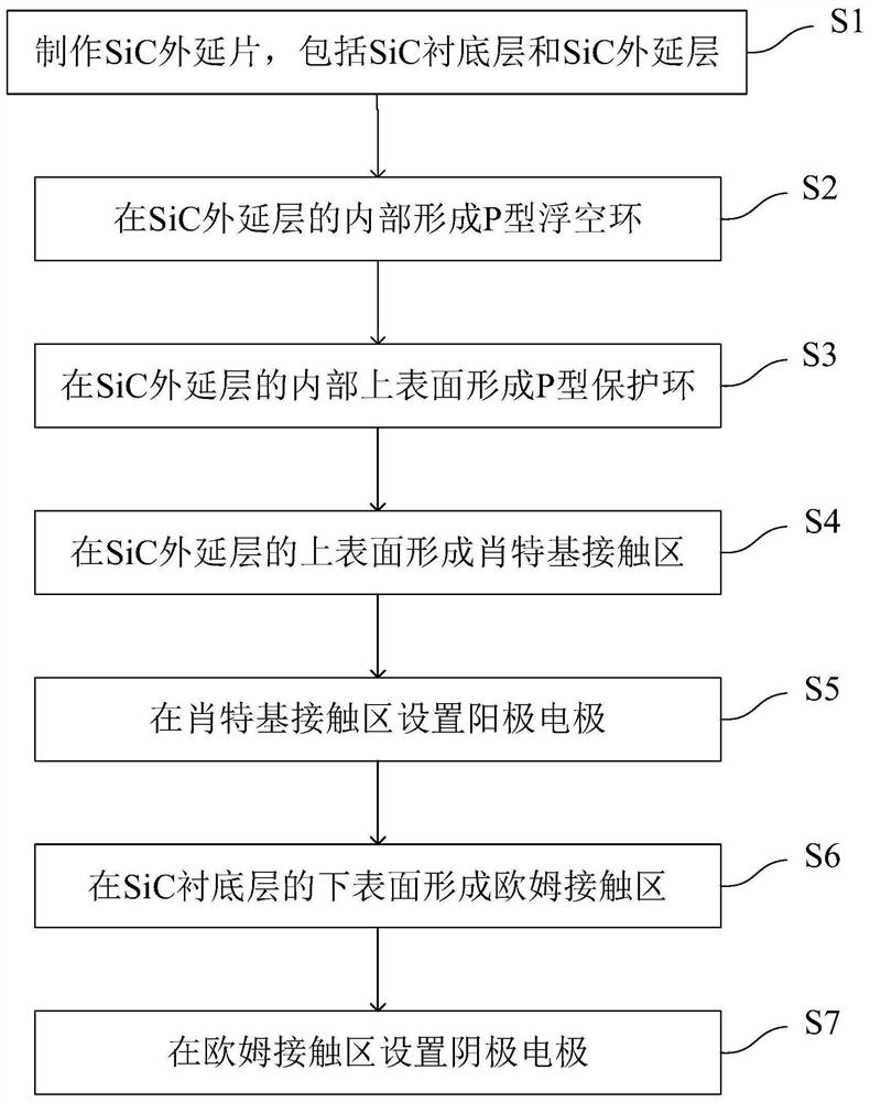
[0041] This embodiment provides a method for preparing a silicon carbide Schottky diode, figure 1 A flowchart of this embodiment is shown. see figure 1 , the preparation method of the present embodiment comprises:
[0042] S1. Fabricate a SiC epitaxial wafer, the SiC epitaxial wafer includes a SiC substrate layer, and an SiC epitaxial layer is provided on the upper surface of the SiC substrate layer.
[0043] S2. Forming a P-type floating ring inside the SiC epitaxial layer.
[0044] S3, forming a P-type guard ring on the inner upper surface of the SiC epitaxial layer.
[0045] S4, forming a Schottky contact region on the upper surface of the SiC epitaxial layer.
[0046] S5, setting an anode electrode on the Schottky contact region.
[0047] Among them, metals such as Pt / Au / Ti can be selected as the anode electrode.
[0048] S6, forming an ohmic contact region on the lower surface of the SiC substrate layer.
[0049] Among them, the metal Au / Ti is evaporated and anneal...
Embodiment 2
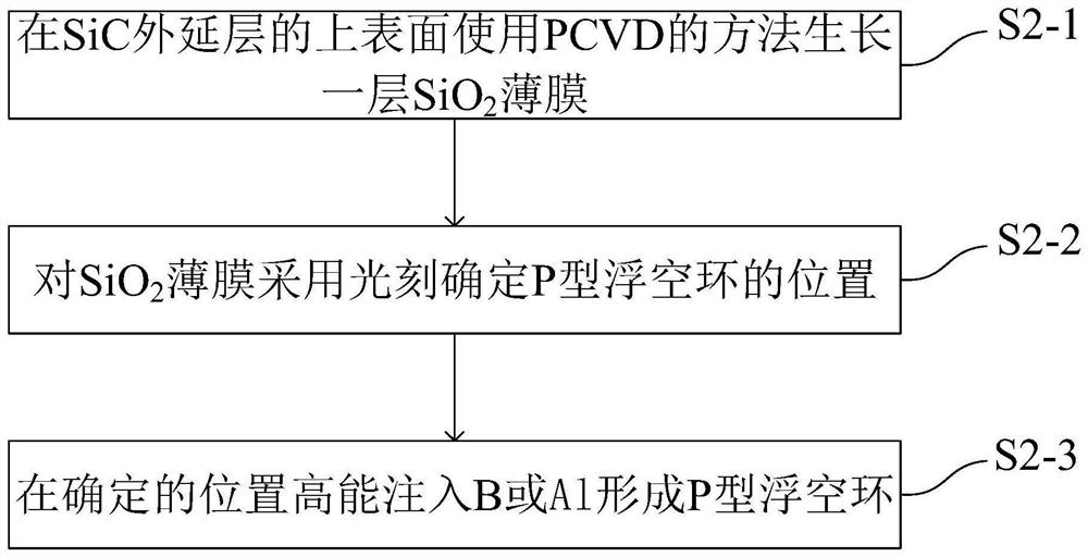
[0053] This embodiment provides a method for preparing a silicon carbide Schottky diode, which is a further improvement on the basis of Embodiment 1. figure 2 The specific steps of forming a P-type floating ring inside the SiC epitaxial layer are shown. see figure 2 , the specific steps include:
[0054] S2-1, growing a layer of SiO on the upper surface of the SiC epitaxial layer by PCVD 2 film.
[0055] Among them, PCVD (Plasma-enhanced Chemical Vapor Deposition), that is, plasma chemical vapor deposition, refers to the method of depositing a thin film on a workpiece at a specific temperature by using a gas containing the constituent atoms of the thin film and using a radio frequency electric field to make the gas form a plasma. This method is widely used in the semiconductor industry.
[0056] S2-2, for the SiO 2 The thin film uses photolithography to determine the position of the P-type floating ring.
[0057] Among them, in the SiO 2 After performing photolithogra...
Embodiment 3
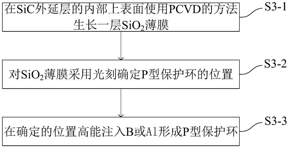
[0063] This embodiment provides a method for preparing a silicon carbide Schottky diode, which is a further improvement on the basis of Embodiment 1 or 2. image 3 The specific steps of forming a P-type guard ring inside the SiC epitaxial layer are shown. see image 3 , the specific steps include:
[0064] S3-1, growing a layer of SiO on the inner upper surface of the SiC epitaxial layer by PCVD 2 film.
[0065] S3-2, for the SiO 2 The thin film uses photolithography to determine the position of the P-type guard ring.
[0066] Among them, in the SiO2 After performing photolithography on the thin film to determine the position of the P-type guard ring, remove the SiO at the position where the P-type guard ring is to be formed. 2 film.
[0067] S3-3. High-energy implantation of B or Al at a certain position to form a P-type protective ring.
[0068] Among them, the energy range of high energy is 200KeV-1MeV.
[0069] In this embodiment, the surface electric field intensi...
PUM
 Abstract
Description
Claims
Application Information


