
A process for making high-efficiency glass passivation chip

A glass passivation and chip technology, which is applied in semiconductor/solid-state device manufacturing, electrical components, circuits, etc., can solve the problems that plague the glass passivation diode chip processing industry, have not achieved obvious results, and wide lateral corrosion, etc., to improve the chip Utilization ratio, increased effective area, and improved forward surge capability

Active Publication Date: 2019-10-25
CHANGZHOUSR SEA ELECTRONICS
View PDF5 Cites 0 Cited by
  • Summary
  • Abstract
  • Description
  • Claims
  • Application Information

AI Technical Summary

Problems solved by technology

Therefore, in the trench corrosion process, the most important control point is the longitudinal corrosion depth. However, since the longitudinal corrosion and lateral corrosion are carried out at the same time, the traditional process has the problem of too wide lateral corrosion after ensuring that the longitudinal corrosion depth meets the requirements.
In response to this problem, measures such as replacing the substrate and reducing the width of the lithography line have not been achieved. This has become a major problem in the glass passivated diode chip processing industry.

Method used

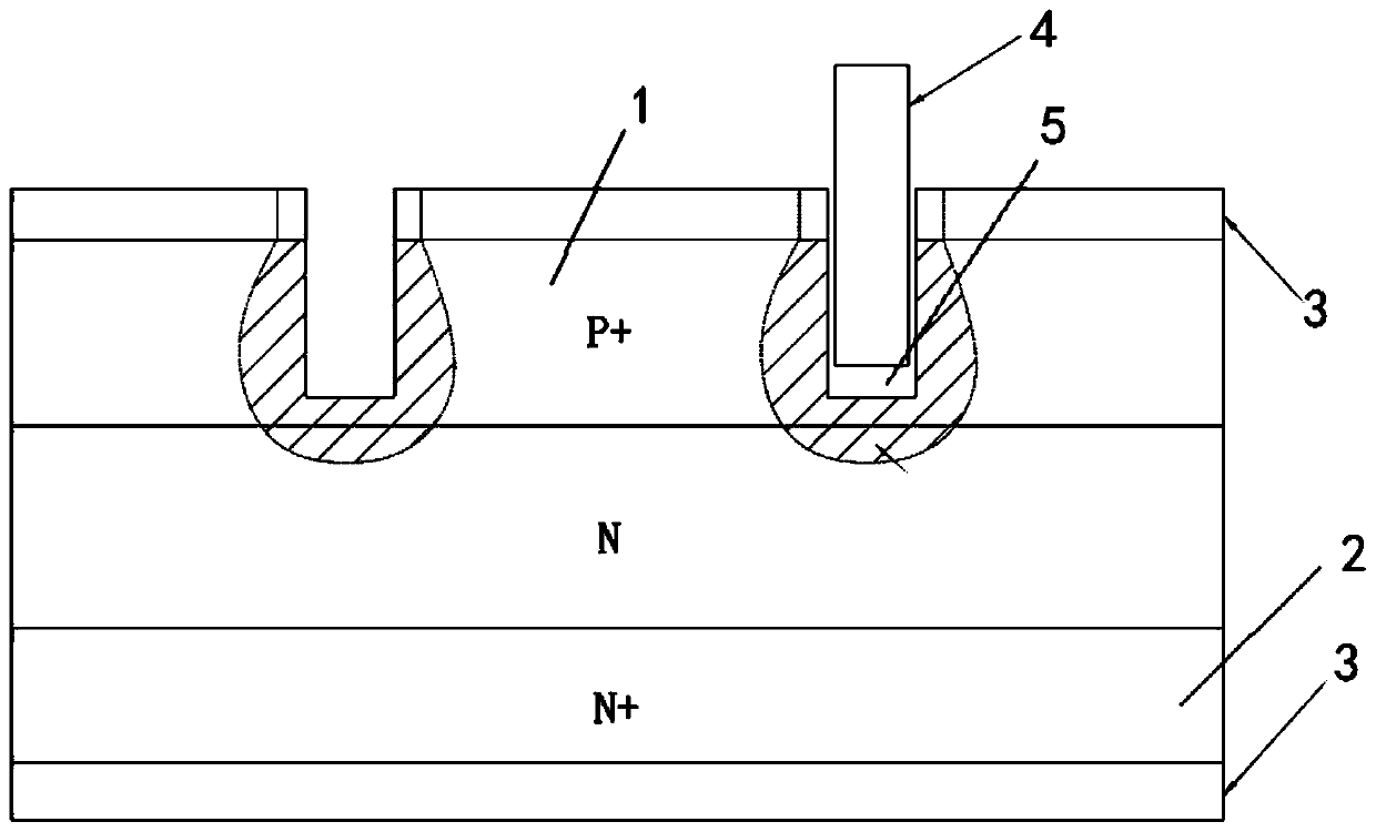
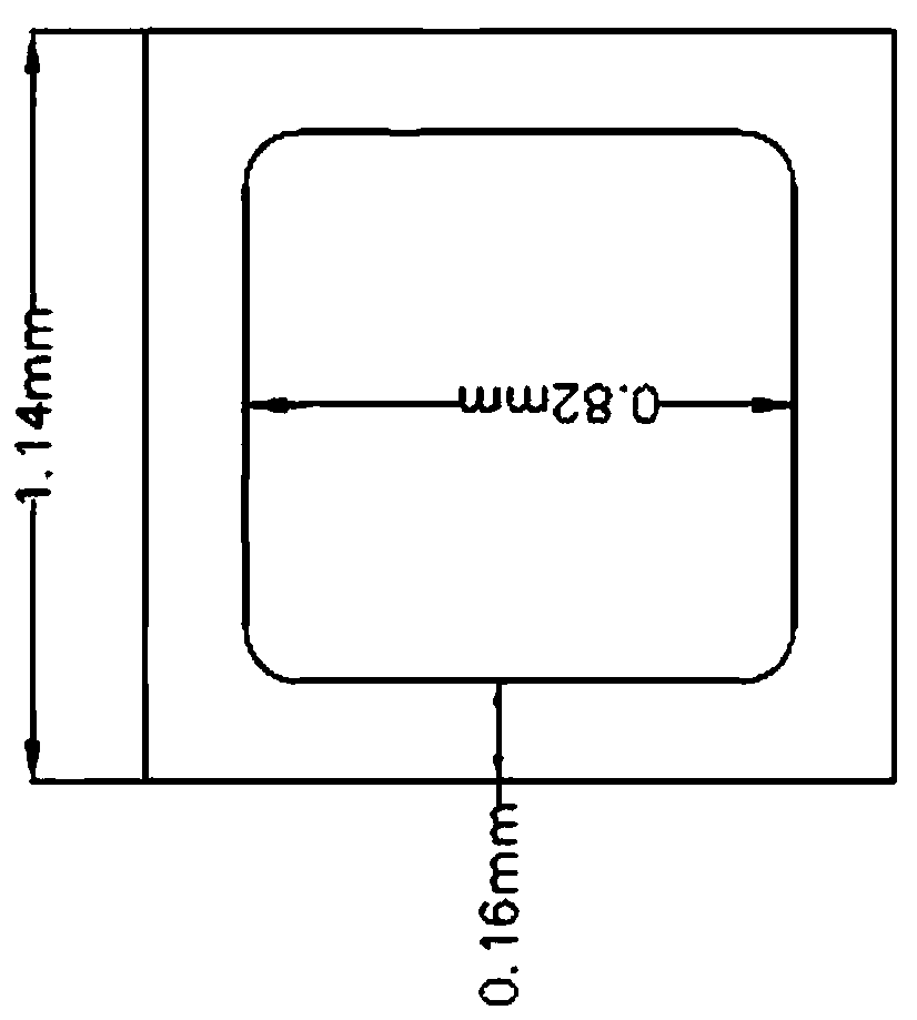
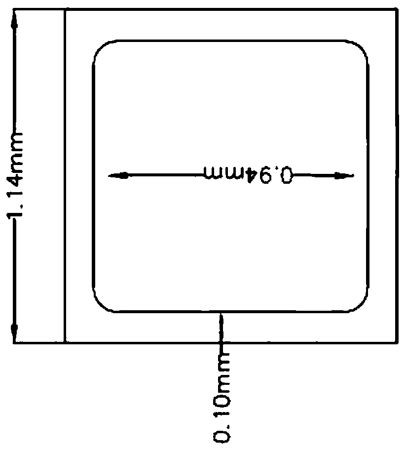

Image

  • A process for making high-efficiency glass passivation chip
  • A process for making high-efficiency glass passivation chip
  • A process for making high-efficiency glass passivation chip

Examples


Embodiment Construction

[0025] In order to make the purpose, technical solutions and advantages of the embodiments of the present invention more clear, the following will clearly and completely describe the technical solutions of the embodiments of the present invention in conjunction with the drawings of the embodiments of the present invention. Apparently, the described embodiments are some, not all, embodiments of the present invention. Based on the described embodiments of the present invention, all other embodiments obtained by persons of ordinary skill in the art without creative efforts shall fall within the protection scope of the present invention.

[0026] Such as figure 1 As shown, a process for making a highly efficient glass passivation chip comprises the following steps,

[0027] S1, respectively covering the boron surface 1 and the phosphorus surface 2 of the silicon wafer with boron and phosphorus diffused with photoresist 3, and performing wireless stripe exposure.

[0028] S2, sel...


PUM

PropertyMeasurementUnit
widthaaaaaaaaaa

Abstract

The invention discloses a high-efficiency glass passivated chip manufacturing process. The process comprises the following steps: a phosphorus surface and a boron surface of a silicon wafer after boron and phosphorus diffusion are covered with photoresist respectively, and no-line exposure is carried out; a diamond scribing knife is selected, cutting is carried out from the middle part of the boron surface of the wafer, cutting and slotting are carried out in the transverse direction and the vertical direction of the boron surface of the wafer, a transverse slot and a vertical slot form a single crystal chip in a surrounding mode, mixed acid corrosion, photoresist removal and cleaning, drying, glass passivation, nickel plating, electric performance test, scribing and cracking are carried out sequentially, and a single diode chip is thus acquired. The diode chip manufactured by the process of the invention has the advantages that the chip size is ensured to be unchanged, the effective area of the chip can be increased obviously, the chip VF is greatly reduced, the forward surge capability is improved, the heating amount is reduced, and the service life of the chip is prolonged; and the effective area of the chip is ensured to be unchanged, the electrical parameter performance of a chip with a smaller size can be ensured to meet requirements, the silicon wafer utilization rate is thus improved, the cost is reduced and the market competition ability is kept.

Description

technical field [0001] The invention relates to a process for manufacturing high-efficiency glass passivation chips. Background technique [0002] The traditional glass passivation chip production process: use photolithography, that is, use photocopying method, to accurately copy the pattern on the photoresist plate on the surface of the diffusion sheet coated with photoresist; Under the protection of the resist, directly perform selective chemical etching on the P+ area of ​​the diffuser, etch through the P-N junction, and the surface of the P-N junction needs to be etched into a mirror surface. [0003] According to the basic characteristics of the diode chip, the longitudinal etching depth of the groove is at least greater than the junction depth during the processing, so as to ensure the optimization of the reverse breakdown voltage of the chip. Therefore, in the trench corrosion process, the most important control point is the longitudinal corrosion depth. However, sin...

Claims


Application Information

Patent Timeline
Patent Type & Authority Patents(China)
IPC IPC(8): H01L21/304H01L21/306H01L21/3105
CPCH01L21/3043H01L21/30604H01L21/3105
Inventor 黄小锋
Owner CHANGZHOUSR SEA ELECTRONICS
Learn More