Nitrogen-containing compounds, electronic components and electronic devices

A nitrogen compound, electronic component technology, applied in electrical components, electrical solid devices, circuits, etc., can solve the problems of only tens of hours of colorization, performance does not meet commercialization requirements, etc., achieve good hole transport characteristics, high Electron tolerance and film-forming properties, effect of large space volume

Active Publication Date: 2022-01-28
SHAANXI LIGHTE OPTOELECTRONICS MATERIAL CO LTD
View PDF8 Cites 0 Cited by
  • Summary
  • Abstract
  • Description
  • Claims
  • Application Information

AI Technical Summary

Problems solved by technology

[0004] At present, in terms of organic electroluminescence materials, the performance of green light materials is relatively good, but for red light and blue light materials, the current performance does not meet the commercialization requirements, and the lifespan in terms of colorization is only dozens of hours

Method used


Image

  • Nitrogen-containing compounds, electronic components and electronic devices
  • Nitrogen-containing compounds, electronic components and electronic devices
  • Nitrogen-containing compounds, electronic components and electronic devices

Examples


Embodiment 1

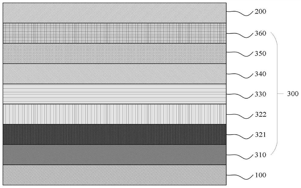
[0247] Embodiment 1: green organic electroluminescent device

[0248] The anode was prepared by the following process: the thickness of ITO was The substrate (manufactured by Corning) was cut into a size of 40mm × 40mm × 0.7mm, and it was prepared into an experimental substrate with cathode, anode and insulating layer patterns by using a photolithography process, using ultraviolet ozone and O 2 :N 2 Plasma surface treatment was performed to increase the work function of the anode (experimental substrate) and to remove scum.

[0249] F4-TCNQ was vacuum evaporated on the experimental substrate (anode) to form a thickness of The hole injection layer (HIL), and NPB is evaporated on the hole injection layer to form a thickness of hole transport layer.

[0250] Compound 1 was vacuum evaporated on the hole transport layer to form a thickness of electron blocking layer.

[0251] On the electron blocking layer, GH-n1:GH-n2:Ir(ppy) 3 Carry out co-evaporation with the ratio of...

Embodiment 2-33

[0255] An organic electroluminescent device was produced in the same manner as in Example 1 except that compounds shown in Table 11 below were used instead of Compound 1 when forming the electron blocking layer.

Embodiment 34

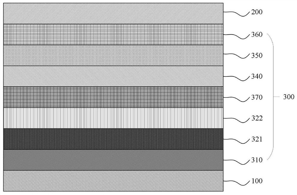
[0276] Example 34: Blue organic electroluminescence device

[0277] The anode was prepared by the following process: the thickness was The ITO substrate (manufactured by Corning) was cut into a size of 40mm × 40mm × 0.7mm, and it was prepared into an experimental substrate with cathode, anode and insulating layer patterns by using a photolithography process, using ultraviolet ozone and O 2 :N 2 Plasma surface treatment was performed to increase the work function of the anode (experimental substrate) and to remove scum.

[0278] F4-TCNQ was vacuum evaporated on the experimental substrate (anode) to form a thickness of The hole injection layer (HIL), and the compound NPB is vacuum-evaporated on the hole injection layer to form a thickness of hole transport layer (HTL).

[0279] Compound 6 was vapor-deposited on the HTL as an electron blocking layer (EBL) with a thickness of

[0280] On the EBL, the compound α,β-ADN is used as the main body, and BD-1 is doped at the sam...


PUM


Abstract

The application provides a nitrogen-containing compound, an electronic component and an electronic device, belonging to the technical field of organic materials. The structure of the nitrogen-containing compound is shown in Chemical Formula 1, and the nitrogen-containing compound can improve the performance of electronic components.

Description

technical field [0001] The present application relates to the technical field of organic materials, and in particular to a nitrogen-containing compound, an electronic component using the nitrogen-containing compound, and an electronic device using the electronic component. Background technique [0002] With the development of electronic technology and the progress of material science, the application range of electronic components for realizing electroluminescence or photoelectric conversion is becoming wider and wider. Such electronic components generally include a cathode and an anode oppositely arranged, and a functional layer arranged between the cathode and the anode. The functional layer is composed of multiple organic or inorganic film layers, and generally includes an energy conversion layer, a hole transport layer located between the energy conversion layer and the anode, and an electron transport layer located between the energy conversion layer and the cathode. ...

Claims


Application Information

Patent Timeline
Patent Type & Authority Patents(China)
IPC IPC(8): C07C211/61C07C211/58C07C255/58C07C211/59C07C211/54C07D209/86C07D307/91C07D213/38C07D333/76C07D209/88C07D405/12C07D409/12H01L51/46H01L51/54
CPCC07C211/61C07C211/58C07C255/58C07C211/59C07C211/54C07D209/86C07D307/91C07D213/38C07D333/76C07D209/88C07D405/12C07D409/12C07C2603/18C07C2603/94H10K85/624H10K85/631H10K85/636H10K85/626H10K85/633H10K85/654H10K85/6576H10K85/6574H10K85/6572Y02E10/549C07D209/82C07C2603/74C07B2200/05C07C2603/28H10K50/181H10K85/615C07D213/16C07D407/10C07C2603/90H10K50/15H10K85/652H10K50/18H10K85/622C07C255/59
Inventor 杨敏南朋
Owner SHAANXI LIGHTE OPTOELECTRONICS MATERIAL CO LTD
Why Eureka
Try Eureka